News & Updates

Blog
•
Proto-BOM in Minutes: How BOM Portal Accelerates Component Selection
Still building BOMs the hard way? Discover how modern workflows can help you create a prototype-ready BOM faster while improving visibility into pricing, availability, and risk.


Blog
•
How to Manage Power Integrity and EMI in Complex Multiboard Systems
This article examines the challenges of maintaining power integrity and controlling EMI in complex multiboard systems. It provides practical strategies for managing return paths, connector transitions, and power distribution across interconnected assemblies.

Blog
•
Agile Teams: From Design Tool to Product Development Platform
Learn how Agile Teams evolves beyond traditional PCB design workflows to support connected product development. This webinar explores how centralized data, collaboration tools, and governance capabilities help teams accelerate delivery while maintaining control.

Blog
•
Benefits of Using an Integrated Design Environment for PCB Development
Using separate tools often creates inefficiencies and increases the risk of mistakes. This article explains how integrated design environments streamline workflows by keeping design data connected and accessible.


Blog
•
Enterprise vs. Midsize PCB Design Software: What Actually Changes at Scale
PCB design challenges change significantly as organizations scale. This article explores the key differences between mid-size and enterprise design environments, from collaboration and governance to data management and workflow automation.


Blog
•
BOM Portal vs BOM Tool: What Changes When You Upgrade
Not all BOM solutions work the same way. This article explains the key differences between BOM tools and BOM portals, and why real-time data and collaboration are becoming essential for modern electronics development.


Blog
•
Altium vs KiCAD: Built to Scale From First Board to Full Product
Starting with a simple board today doesn't mean your next project will stay simple. Learn how Altium Designer and KiCAD compare when designs become more complex, teams get larger, and products move toward manufacturing.

Blog
•
Eliminate the Design-to-Production Gap with Agile Teams + Duro
Learn how Agile Teams and Duro connect design and production workflows through a unified system of record. This webinar shows how structured change management and automated data synchronization help teams reduce errors and accelerate product releases.

Blog
•
Agile Hardware Development: How to Scale Speed Without Losing Control
Agile hardware development isn’t just about working faster, it’s about working together in real time. This article explores how shared environments for ECAD, MCAD, sourcing, and requirements management eliminate handoff delays and improve decision-making across teams.


Blog
•
How Reusable Parameters in Requirements Reduce Errors and Speed Up Iterations
Verification becomes much easier when requirements and system performance data stay connected automatically. This article explains how reusable parameters and V&V rules help teams detect violations earlier and validate designs with greater confidence.


Blog
•
Complex Engineering Projects Leverage Multiple ECAD/MCAD Formats
This article explores how modern engineering teams manage complex projects involving multiple ECAD, MCAD, and manufacturing file formats across distributed workflows. It highlights the importance of design authority, disciplined revision control, and bidirectional collaboration to ensure accurate integration between PCBs and mechanical systems.


Blog
•
Avoid Costly Interconnect Errors: Essential Multiboard PCB Layout Strategies for Reliable Designs
Complex multiboard designs demand more than just connecting boards together. They require every interface to work flawlessly under real-world conditions. Discover how better pin assignments, return paths, and mechanical planning can dramatically improve reliability and reduce rework.


Blog
•
High-Speed PCB Design Tips
Essential tips for high-speed PCB designs, and when you need to start being concerned about how and where you route your traces.
Blog
•
MIDs Make a Comeback as Vertical SMD Modules for Your PCB
If you've ever wanted to mount components vertically, but without the expense of a flex section this article is for you. You can use an MID in your PCB.
Blog
•
Everything You Need to Know about Conformal Coating
Explore the basics of conformal coating with us. Conformal coating is a protective layer applied to electronic circuits to guard against environmental factors such as moisture and dust.

Blog
•
Introduction to Open Source Laptop Project
We have started a very exciting journey into the creation of an open source laptop project. This project will be an ongoing one, with our community able interactively participate. By utilizing Altium 365 users will be able to view, comment on, and download design files. This will be a great learning experience for new and experienced PCB designers.

Blog
•
Mechanical and Electrical Design Come Together With Altium’s MCAD CoDesigner
Electronics designers working in small design houses or in large enterprises often encounter a common set of challenges when interfacing with mechanical designers. Continue reading to learn how you can best interface with your mechanical designer to get your projects out the door fast!
Blog
•
Ebook: Routing High-Density Interconnects with Reliable Microvias
HDI PCBs take a particular approach to routing interconnects through multiple layers to ensure reliability during fabrication, assembly, and operation. The critical structure that enables this is microvias, which are prone to failure if not designed properly. In this e-book, readers will receive an initial look at the reasons microvia reliability has come into the spotlight and why HDI PCB designers put reliability first when routing through microvias.

Blog
•
IPC-2221 Calculator for PCB Trace Current and Heating
Aside from impedance and annular ring calculations, one of the other major formulas specified in the IPC 2221 standard relates temperature rise, trace width, and trace current. THere is also the IPC-2152 standard, both include this guidance on designing for thermal reliability, but which standard should we use?
Blog
•
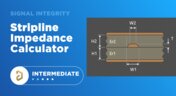
Stripline Impedance Calculator
Striplines provide some advantages over microstrips as they take advantage of natural shielding and coupling from nearby ground plane layers. Although they tend to experience higher losses due to total confinement in the dielectric, they can be thinner due to the high dielectric constant used in internal layers of a PCB. Use our free impedence calculator to help you determine the correct width needed to hit a target impedance.

Blog
•
Which Types of Opto-Isolators Are Right For Your Signal?
An optoisolator is a cool electronic device that can be used to pass information between a diode without passing an electrical current. There are many great applications for these, but do you know which one is right for you?

Blog
•
Properties panel document options in SCH editors
The Properties panel provides access to the properties of documents and objects. The contents of the panel change depending on the active document or the selected object. This blog will quickly go over some of need to know options around the properties panel in the schematic document.

Blog
•
The High-Speed PCB Stackup Design Challenge
Even with all the good guidelines out there for high speed design, there are particular aspects of stackup construction and their relation to building boards that get overlooked. This blog is goes beyond just the typical SI/PI guidelines and looks at these problems from more of an engineering perspective.
Blog
•
Everything You Need to Know About Stitching Vias
Stitching vias are something you often see spread around the surface layer of a PCB, but what are they? and should you be using them? In this guide, we'll go over some of the standard uses of stitching vias and when they should be used in a PCB.
Blog
•
PCB Stackup Basics
In comparison to the build-up of a PCB, the stackup is more concerned with the electrical type of each layer, that is are we working with signals, power, or ground. Continue reading to learn how you can optimize your layer stack.

Blog
•
Multi-board and Harness Design Capability in Altium Designer 23
Altium’s VP of marketing Lawrence Romine discusses the multi-board and harness design capabilities coming in Altium Designer 23.

Blog
•
Controlled ESR Capacitors: Should You Use Them for Power Integrity?
Controlled ESR capacitors are important for power integrity in your design as they can help smooth out the PDN impedance spectrum in your high speed PCB.

Blog
•
How Does the Package PDN Impact Power Integrity?
Whenever we say something to the effect of “components can’t work without a correctly designed PCB,” we only have to look at component packaging for evidence. It is true that component packages come with parasitics that affect signal integrity, but there is one area that we don’t often look at in terms of component packaging: power integrity.


Your search returns no results.


