News & Updates
Blog
•
Proto-BOM in Minutes: How BOM Portal Accelerates Component Selection
Still building BOMs the hard way? Discover how modern workflows can help you create a prototype-ready BOM faster while improving visibility into pricing, availability, and risk.


Blog
•
How to Manage Power Integrity and EMI in Complex Multiboard Systems
This article examines the challenges of maintaining power integrity and controlling EMI in complex multiboard systems. It provides practical strategies for managing return paths, connector transitions, and power distribution across interconnected assemblies.

Blog
•
Agile Teams: From Design Tool to Product Development Platform
Learn how Agile Teams evolves beyond traditional PCB design workflows to support connected product development. This webinar explores how centralized data, collaboration tools, and governance capabilities help teams accelerate delivery while maintaining control.

Blog
•
Benefits of Using an Integrated Design Environment for PCB Development
Using separate tools often creates inefficiencies and increases the risk of mistakes. This article explains how integrated design environments streamline workflows by keeping design data connected and accessible.


Blog
•
Enterprise vs. Midsize PCB Design Software: What Actually Changes at Scale
PCB design challenges change significantly as organizations scale. This article explores the key differences between mid-size and enterprise design environments, from collaboration and governance to data management and workflow automation.


Blog
•
BOM Portal vs BOM Tool: What Changes When You Upgrade
Not all BOM solutions work the same way. This article explains the key differences between BOM tools and BOM portals, and why real-time data and collaboration are becoming essential for modern electronics development.

Blog
•
Altium vs KiCAD: Built to Scale From First Board to Full Product
Starting with a simple board today doesn't mean your next project will stay simple. Learn how Altium Designer and KiCAD compare when designs become more complex, teams get larger, and products move toward manufacturing.

Blog
•
Eliminate the Design-to-Production Gap with Agile Teams + Duro
Learn how Agile Teams and Duro connect design and production workflows through a unified system of record. This webinar shows how structured change management and automated data synchronization help teams reduce errors and accelerate product releases.

Blog
•
Agile Hardware Development: How to Scale Speed Without Losing Control
Agile hardware development isn’t just about working faster, it’s about working together in real time. This article explores how shared environments for ECAD, MCAD, sourcing, and requirements management eliminate handoff delays and improve decision-making across teams.


Blog
•
How Reusable Parameters in Requirements Reduce Errors and Speed Up Iterations
Verification becomes much easier when requirements and system performance data stay connected automatically. This article explains how reusable parameters and V&V rules help teams detect violations earlier and validate designs with greater confidence.


Blog
•
Complex Engineering Projects Leverage Multiple ECAD/MCAD Formats
This article explores how modern engineering teams manage complex projects involving multiple ECAD, MCAD, and manufacturing file formats across distributed workflows. It highlights the importance of design authority, disciplined revision control, and bidirectional collaboration to ensure accurate integration between PCBs and mechanical systems.


Blog
•
Avoid Costly Interconnect Errors: Essential Multiboard PCB Layout Strategies for Reliable Designs
Complex multiboard designs demand more than just connecting boards together. They require every interface to work flawlessly under real-world conditions. Discover how better pin assignments, return paths, and mechanical planning can dramatically improve reliability and reduce rework.


Blog
•
Pi.MX8 Project - Board Layout Part 1
Our exploration of the Pi.MX8 open-source computer module project progresses. In this third chapter, our focus shifts to the PCB layout preparation of the board. Key topics include defining the layerstack and component break-out routing.

Blog
•
PCB CoDesign Whitepaper
Design faster together with the innovative PCB CoDesign feature, exclusively available in Altium Designer. This cutting-edge functionality seamlessly integrates schematic and PCB design, facilitating concurrent work by multiple engineers on the same project. Learn more about this groundbreaking feature in our comprehensive manual.

Blog
•
How to Test Suspect Electronic Components
Electronic components power nearly everything in our modern lives. However, as long as there are buyers for parts, counterfeiters will persist in their endeavors. Financial losses resulting from fake components are challenging to ascertain due to enforcement limitations and the difficulty in collecting data on the issue. In this article, we demonstrate how to test and verify components in batch orders.

Blog
•
The Positive Impact of Supply Chain Visibility on Design to Cost
With increased electronics supply chain visibility, you can develop better products faster and align perfectly with budget constraints early on. Here’s why.

Blog
•
What Most Agile "Gurus" Get Wrong About Hardware Development
Explore common myths about Agile hardware development and learn how to adapt Agile principles for hardware projects.

Blog
•
Design Phase – Lid Assembly Electronics Part 2
We are going deeper into lid assembly electronics in our Open Source Laptop project. In this chapter we will tackle the PCB design of the webcam board and show you how to deal with some expected challenges, such as overall small form factor of the board or breaking out the microscopic webcam image sensor.

Blog
•
Compare Commercial Altium 365 vs Altium 365 GovCloud
If you're trying to understand how commercial Altium 365 differs from Altium 365 GovCloud, you're in the right place. Click to grasp the unique features of each.

Blog
•
5 Ways Hardware Development Is Just… Different
Explore the challenges and strategies of implementing Agile methodology in electronics hardware development. Understand key differences between hardware and software development within the Agile framework.

Blog
•
Flexible Circuit Assembly: Thinking Through Component Placement
The flexible circuits are ideal for applications where a thin, small, and lightweight PCB is needed. However, in such cases, challenges in assembly and fabrication often arise. This article delves into these challenges, focusing on component selection and placement and how they can significantly impact the performance of the flexible circuit in its intended application.
Blog
•
Coding Your Own Networked Test Equipment
Have you ever performed manual tests? If your answer is yes, you're likely aware of how laborious and time-consuming the entire process can be. Allow us to introduce you to the realm of test equipment automation. Our new step-by-step guide empowers you to write code that seamlessly configures your networked test equipment, all from the convenience of your computer.
Blog
•
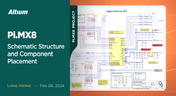
Pi.MX8 Project – Schematic structure and component placement
We are advancing with our brand new Pi.MX8 Project. In this chapter, we delve deeper into two crucial aspects: the overall schematic and component placement on the PCB board. Don't hesitate to check it out. Additionally, you can follow this project through our workspace; the link is provided within the article.
Blog
•
Redefine PCB Boundaries with HDI Design
Dive into the world of High-Density Interconnect (HDI) design to enhance your projects. Explore heightened signal integrity, improved reliability, and the seamless integration of advanced technologies - all within compact and lightweight designs. Discover more about HDI on our updated feature page.
Blog
•
OrCAD Design Collaboration in Altium 365
Ready to start collaborating on your OrCAD projects in a multi-CAD environment? Check how you can use Multi-CAD File Support in Altium 365 in practice.
Blog
•
The Critical Role of Constraint-Based PCB Design in Modern Electronics
A constraint-based approach to PCB design is crucial in today's electronics industry. This article delves deeper into this complex and interesting topic, exploring various types of constraints, their advantages, and providing guidance on implementing them into your PCB design process.
Blog
•
Pi.MX8 Project – Introduction and Overview
Do you have extensive knowledge about the Pi.MX8 module? We're excited to introduce a new series of articles focusing on an innovative approach to utilizing this module. In this inaugural chapter, we provide insights into the preparation for this project and detail the elements that will be used.

Blog
•
How to 'Shift Left' and Connect Procurement and Engineering? Altium 365 BOM Portal Step-by-Step
Learn why BOM management is critical for both procurement managers and electronic engineers. Altium 365 BOM Portal helps to bridge the gap between these worlds. Discover how!





Your search returns no results.


