News & Updates

Blog
•
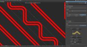
Stack-Up to Success: Avoid the Pitfalls
"Stack‑Up to Success" highlights how a carefully planned PCB stack‑up is foundational to preventing warpage, managing impedance, and avoiding manufacturing delays by clearly communicating layer construction, materials, and tolerance requirements to fabricators.
Blog
•
IC Components Explained: A Comprehensive Guide to Integrated Circuits
Gain a clear understanding of the fundamental elements within integrated circuits. This guide examines their structure, function, and role in system performance, knowledge that’s vital for anyone involved in sourcing or developing electronic designs.
Blog
•
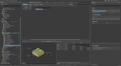
Ensuring Precise Connector Alignment in Multi‑Board Manufacturing
Misaligned connectors can cause major issues in multi-board assemblies. In this article, David Marrakchi shows how Altium’s 3D tools help detect and fix alignment problems early in the design process.

Blog
•
Getting Started with the Renesas RA8D1 Evaluation Kit and Edge AI
Dive into the power of Renesas’ RA8D1 MCU using the EK‑RA8D1 evaluation kit. Learn how to train, test, and deploy image‑based detection models seamlessly with Edge Impulse, and kickstart your embedded vision AI projects in minutes.


Blog
•
How to Effectively Use Jira for Hardware Development Projects
Originally built for software development, Jira has become a popular tool for agile project management across various industries. Our new article explores how hardware teams can leverage core Jira features and adapt agile principles to suit the unique needs of hardware development.


Blog
•
Building Supply Chain Resilience: Transforming BOM Management for Modern Electronics
Discover why top electronics companies are replacing spreadsheets with purpose-built BOM management solutions. This whitepaper outlines the risks of outdated methods, offers a readiness checklist, and explores how BOM Portal helps teams cut costs, reduce risk, and speed up development with smarter, data-driven workflows.

Blog
•
Material and Process Considerations That Influence Performance
Material and process choices play a key role in high-performance PCB design. This article highlights how stack-up configuration, substrate selection, and lamination strategy impact signal integrity, reliability, and manufacturability.


Blog
•
How to Make Your PCB Layout AOI and X-Ray Friendly
Designing for inspection is key to reliable manufacturing. This article covers practical PCB layout tips to optimize your board for AOI and X-ray inspection helping you reduce defects, false positives, and production delays.


Blog
•
Understanding Systems Engineering
Read our brand-new article where we explore the key areas of an engineering project and the different stages of electronic product development from a project execution perspective. From initiation and planning to design, development, validation, testing, and certification, we walk you through each phase to help you understand how successful electronic products are brought to life.


Blog
•
PCB First-Pass Yield: Small Decisions That Make a Big Difference
This article highlights how seemingly minor layout choices like trace spacing, component footprints, or stack-up details can dramatically impact whether a board passes fabrication and assembly the first time.

Blog
•
Implementing Design for Supply Chain Principles in Electronic Product Development
Designing with supply chain principles in mind helps you avoid delays, reduce costs, and ensure manufacturability. This article outlines practical strategies for component selection, sourcing, and lifecycle management to make your designs more resilient and production-ready.

Blog
•
How Engineering Project Management Tools Are Changing Engineering Teams’ Productivity
Engineering project management tools play a critical role in managing timelines, resources, and cross-disciplinary coordination. This article breaks down the most impactful systems for improving execution and team performance.

Blog
•
7 Ways to Catch Rules & Constraints Early – Checklist
Discover seven actionable ways to spot and fix rules and constraint issues before they derail your PCB project. Using Altium Designer Agile, these tips help you build more manufacturable and reliable boards with fewer iterations.

Blog
•
Do You Need an IPC-D-356 Netlist?
If your output package is Gerber-based, adding an IPC-D-356 netlist can dramatically improve how your design is reviewed and validated for production. Here’s when it matters, what it contains, and how to generate it quickly in Altium.

Blog
•
How Agile BOM Management Helps You Lock in Pricing Before Market Shifts
When engineering and procurement work from different BOM versions, delays and cost surprises follow. Learn how agile BOM management brings teams onto one connected BOM so they can respond fast, manage risk, and lock pricing early.

Blog
•
Flexible Circuits: Enhancing Performance with Shielding, Heat Dissipation, and Stiffeners
A flex circuit can look perfect on paper and still fail in the real world due to EMI, hot spots, or mechanical strain. This article breaks down how shielding, thermal planning, and stiffeners help deliver designs that stay reliable over time.

Blog
•
Avoid These Top 3 Power Distribution Failures in PCB Design
Power distribution issues can silently undermine your PCB’s reliability. This article uncovers the top three failure modes and shows how Power Analyzer by Keysight helps you catch them early in the design phase and how Altium Agile Teams turns those checks into structured team action.

Blog
•
From BOM to Requirements and Back: Building Sourcing Constraints Into Specs
When engineering and procurement remain disconnected, supply-chain problems will sneak up on you. This guide argues convincingly: embed sourcing constraints into your requirements from day one, and avoid costly rework down the line.

Blog
•
Understanding Power Integrity in PCB Design: Power Analyzer by Keysight Whitepaper
Power integrity is the backbone of reliable PCB design. This whitepaper explains how to analyze and optimize voltage drop, current density, and grounding directly within Altium Designer Agile using the Power Analyzer by Keysight.
Blog
•
How to Manage ECAD Libraries for Consistent PCB Layout Design
Strong hardware starts with strong libraries. Discover how disciplined ECAD-library management dramatically improves design consistency and accelerates every stage of your PCB workflow.

Blog
•
High Speed PCB Design Review: Signal Integrity Questions You Should Always Ask
As data rates increase, the risks hidden in your layout grow with them. This quick guide highlights the critical SI checkpoints that can save you from late-stage surprises and redesigns. If you design high-speed boards, you’ll want to read this before your next review.

Blog
•
Supplier Negotiation: Turn Market Data Into Your Best Negotiation Tool
Don’t walk into supplier talks blind. Use market data to benchmark quotes, check lead times and uncover alternate parts. This article shows how visibility can shift the balance and de-risk your BOM.

Blog
•
Via-in-Pad in Rigid-Flex Designs: When Space Is Tight, Details Matter
Designing rigid-flex boards is like solving a 3D puzzle of materials, bends and tight spaces, and via-in-pad might just be the piece you need. Dive into how and when to use via-in-pad in rigid-flex designs, and what to watch out for from fabrication to field reliability.
Blog
•
Wearable Electronics: Innovations, Challenges & Future Trends
This whitepaper examines how next-generation wearable electronics are evolving through advancements in flexible and rigid-flex design, smart materials, AI, energy innovations, and connectivity. Discover what’s required to transform early prototypes into scalable, reliable products across healthcare, sports, defense, fashion, and enterprise applications.

Blog
•
Streamlining Component Selection for Long Product Lifecycles
Electronic parts may now cycle from launch to end-of-life in just a few years, but many systems are expected to serve for 10–20+ years. Here’s how to build a component selection process that aligns engineering, procurement and design for longevity and stability.

Blog
•
Using ECAD Software to Track Part Availability During PCB Design
As component lead-times extend and obsolescence becomes a persistent threat, PCB projects demand more than schematic capture and layout tools alone. This article details how ECAD software with embedded supply-chain intelligence can: unify engineering and procurement teams; provide visibility into stock levels, lead times and alternates; and enable proactive risk mitigation within the design loop.

Blog
•
PCB Design Data Management Tips for Multi-Board Projects
In complex electronic systems, managing data from multiple printed circuit boards can quickly become a logistical challenge. This article outlines a structured workflow for handling both board-level and assembly-level design outputs, ensuring clarity and consistency across fabrication, assembly and product-level documentation.
















Your search returns no results.


