News & Updates

Blog
•
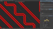
Stack-Up to Success: Avoid the Pitfalls
"Stack‑Up to Success" highlights how a carefully planned PCB stack‑up is foundational to preventing warpage, managing impedance, and avoiding manufacturing delays by clearly communicating layer construction, materials, and tolerance requirements to fabricators.
Blog
•
IC Components Explained: A Comprehensive Guide to Integrated Circuits
Gain a clear understanding of the fundamental elements within integrated circuits. This guide examines their structure, function, and role in system performance, knowledge that’s vital for anyone involved in sourcing or developing electronic designs.
Blog
•
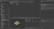
Ensuring Precise Connector Alignment in Multi‑Board Manufacturing
Misaligned connectors can cause major issues in multi-board assemblies. In this article, David Marrakchi shows how Altium’s 3D tools help detect and fix alignment problems early in the design process.

Blog
•
Getting Started with the Renesas RA8D1 Evaluation Kit and Edge AI
Dive into the power of Renesas’ RA8D1 MCU using the EK‑RA8D1 evaluation kit. Learn how to train, test, and deploy image‑based detection models seamlessly with Edge Impulse, and kickstart your embedded vision AI projects in minutes.


Blog
•
How to Effectively Use Jira for Hardware Development Projects
Originally built for software development, Jira has become a popular tool for agile project management across various industries. Our new article explores how hardware teams can leverage core Jira features and adapt agile principles to suit the unique needs of hardware development.


Blog
•
Building Supply Chain Resilience: Transforming BOM Management for Modern Electronics
Discover why top electronics companies are replacing spreadsheets with purpose-built BOM management solutions. This whitepaper outlines the risks of outdated methods, offers a readiness checklist, and explores how BOM Portal helps teams cut costs, reduce risk, and speed up development with smarter, data-driven workflows.

Blog
•
Material and Process Considerations That Influence Performance
Material and process choices play a key role in high-performance PCB design. This article highlights how stack-up configuration, substrate selection, and lamination strategy impact signal integrity, reliability, and manufacturability.


Blog
•
How to Make Your PCB Layout AOI and X-Ray Friendly
Designing for inspection is key to reliable manufacturing. This article covers practical PCB layout tips to optimize your board for AOI and X-ray inspection helping you reduce defects, false positives, and production delays.


Blog
•
Understanding Systems Engineering
Read our brand-new article where we explore the key areas of an engineering project and the different stages of electronic product development from a project execution perspective. From initiation and planning to design, development, validation, testing, and certification, we walk you through each phase to help you understand how successful electronic products are brought to life.


Blog
•
PCB First-Pass Yield: Small Decisions That Make a Big Difference
This article highlights how seemingly minor layout choices like trace spacing, component footprints, or stack-up details can dramatically impact whether a board passes fabrication and assembly the first time.

Blog
•
Implementing Design for Supply Chain Principles in Electronic Product Development
Designing with supply chain principles in mind helps you avoid delays, reduce costs, and ensure manufacturability. This article outlines practical strategies for component selection, sourcing, and lifecycle management to make your designs more resilient and production-ready.
Blog
•
Best Tools For PCB DFM Checks
Want to catch manufacturability issues before they turn into expensive delays? Discover the essential DFM tools from real-time checks to post-layout analysis that help you get your PCB right the first time.

Blog
•
Eliminate Your Design Friction with Agile Teams
Design friction from scattered data and disconnected tools slows down PCB development and leads to rework. This webinar shows how Agile Teams streamlines collaboration, aligns domains, and helps teams deliver faster with fewer errors.

Blog
•
What Is an Integrated Design Environment for Electronics?
Using multiple disconnected tools slows down PCB development and increases the risk of errors. This article shows how an integrated environment keeps all design data connected, enabling faster workflows and fewer late-stage issues.

Blog
•
What is the Best Cloud PCB Design Software?
Not all cloud PCB tools are created equal, especially when design complexity increases. This article breaks down key differences between cloud-native and hybrid solutions, helping engineers choose the right approach for performance and scalability.

Blog
•
From Rework to Revenue: Digital PCB DFMA
This article explores how traditional, manual DFMA workflows lead to costly rework, delays, and poor collaboration across engineering teams. It shows how a connected, digital approach enables better data integrity, faster design cycles, and improved manufacturing outcomes.

Blog
•
Introducing Octopart Discover: From Part Search to Solutions Discovery
Octopart has announced Octopart Discover, a new platform that shifts electronic component search toward system-level solution discovery. The tool connects design intent with relevant options, enabling engineers to evaluate tradeoffs and identify the best-fit solutions more efficiently.

Blog
•
How to Choose the Right Components for Your BOM
A strong BOM can make the difference between smooth production and costly delays. Discover a practical approach to choosing components that stay available, meet compliance requirements, and keep your project on schedule.

Blog
•
From Scattered Requirements to Confident Product Development
See how the Requirements Portal transforms disconnected requirements into a single, live source of truth that engineers can trust at every stage of a project! Real customer stories in the article prove it’s already helping teams cut down on rework and bring products to market faster.

Blog
•
What is the Best PCB Design Tool For Students?
Students need PCB software that’s intuitive, affordable, and useful for building real skills. This article compares the strengths and weaknesses of leading design tools, from hobbyist platforms to industry-standard software.

Blog
•
What Is Collaborative Engineering?
Collaborative engineering is all about breaking down silos so electrical, mechanical, and sourcing teams can work as one with shared data and real-time updates. This article shows how that approach helps you spot issues early, reduce rework, and get products out the door with fewer surprises.

Blog
•
Bend Reliability: How Trace Geometry and Materials Impact Flex Lifespan
Focused on durability under repeated mechanical stress, this piece details how routing strategy, copper thickness, adhesive systems, and bend radius selection determine flex lifespan. Engineers will find actionable recommendations for reducing strain concentration and improving long-term performance in high-cycle applications.

Blog
•
PCB Design Process: The EDA Design Approach
Dive into how a modern EDA workflow transforms PCB design by linking electrical, mechanical, and manufacturing requirements from idea to final release. With constraint‑driven integration, you can cut down on respins and bring better boards to market faster.
Blog
•
Getting Started for Mechanical Engineers
Explore our collection of MCAD Collaboration walkthroughs, where you’ll discover how to synchronize mechanical constraints and keepouts, maintain traceability with advanced history and revision control, and streamline electromechanical connectivity through harness synchronization. These topics and many more are covered in this article.

Blog
•
Are Your ECAD Tools Holding Back Engineers’ Productivity?
The article highlights that productivity issues often stem from tool limitations rather than engineer effort, especially as project complexity grows. ECAD tools that offer clear version control, cross-discipline integration, and workflow awareness are key to sustaining efficiency.
Blog
•
How Integrated PCB Design Cuts Development Time for Complex Electronics
Fewer tool handoffs, fewer errors, and smoother collaboration that’s the power of integrated PCB design. Learn how unifying your design environment can cut development time and help you deliver complex electronics faster.

Blog
•
Registration Challenges in UHDI: Why Fabrication Tolerances Matter in Your Layout
As UHDI structures shrink, achieving accurate layer-to-layer registration becomes less forgiving than ever. Learn why fabrication tolerances matter so much in ultra-fine geometries and how to design with registration limits in mind from the start.
















Your search returns no results.


