News & Updates

Blog
•
Who Needs Integrated Electronic Component Search
Finding the right component shouldn't mean searching through dozens of websites and datasheets. This article shows how integrated component search helps engineers select parts faster while reducing sourcing risks and design delays.


Blog
•
How BOM Portal Supports R&D and Procurement with DFM & DFC Analysis Throughout the Entire Product Lifecycle
The best sourcing decisions happen when procurement is involved early. This webinar demonstrates how BOM Portal gives both engineering and procurement access to live lifecycle, pricing, compliance, and availability data to drive smarter decisions from prototype through production.

Blog
•
How to Design a PCB: From Schematic Capture to Manufacturing
This article walks through the complete PCB design workflow, from schematic capture and component selection to layout, design reviews, and manufacturing documentation. It highlights the key decisions at each stage that help engineering teams produce reliable, manufacturable products.

Blog
•
5 Power Integrity Myths: AC Edition
The biggest threat to your power integrity might be outdated design advice. This article challenges five common AC power integrity myths and shows what really matters when designing today's high-speed PCBs.


Blog
•
Your Design Data Has Zero Defense
Your design data may be more exposed than you think. This webinar shows how to identify common security gaps and secure engineering workflows with centralized access control and governance.


Blog
•
Flex Circuit Coverlay: Design with Lamination Processes In Mind
Your flex PCB may look perfect in CAD but coverlay doesn't stay perfectly still during manufacturing. This article reveals why designing for lamination behavior is one of the most important steps in building reliable flex circuits.


Blog
•
Integrated PCB Design vs. Legacy Point Tools: What’s the Real Cost?
As hardware development grows more collaborative, disconnected point tools can introduce data inconsistencies, traceability gaps, and costly coordination challenges. This article examines how integrated PCB design environments connect design, mechanical, supply chain, and review workflows to improve efficiency throughout the product lifecycle.

Blog
•
Make Better Design Decisions with Signal and Power Integrity Insight
Signal integrity and power integrity are closely connected, with problems in one often affecting the other as designs become faster and more complex. This webinar explains how integrated analysis workflows help engineers evaluate PDN performance, identify potential issues early, and improve overall design quality.

Blog
•
Optimizing Your Electronics Product Design Workflow and Eliminating Bottlenecks
Every manual handoff adds time and risk to the product development process. This article shows how modern design workflows automate routine tasks, improve data visibility, and help engineering teams focus on innovation instead of administration.

Blog
•
Avoid Cross-Board Signal Integrity Issues in High-Performance Multiboard PCB Designs
Your signal may be perfect on the PCB and fail the moment it crosses a connector. This article explores the hidden SI challenges in multi-board systems and how engineers can eliminate them before they become costly debugging sessions.


Blog
•
Proto-BOM in Minutes: How BOM Portal Accelerates Component Selection
Still building BOMs the hard way? Discover how modern workflows can help you create a prototype-ready BOM faster while improving visibility into pricing, availability, and risk.

Blog
•
6 Areas Your PCB Design Reviews Should Focus On
Learn the six essential topics every electronics team should address in design reviews to improve quality, avoid surprises and bring products to market faster.

Blog
•
What Is BOM Management? A Practical Guide to Avoiding Costly Part Mismatches
From design to production, effective Bill of Materials (BOM) management is critical to ensuring smooth collaboration between engineering, procurement, and manufacturing teams. In this practical guide, we break down proven strategies for structuring, maintaining, and synchronizing your BOM to prevent costly mistakes and accelerate time-to-market.

Blog
•
Requirements Portal Introductory Tutorials
This series of guided demos shows how the Altium Requirements Portal transforms scattered requirement spreadsheets and emails into traceable, version-controlled data that stays aligned with your PCB design efforts.

Blog
•
Bridging the Gap: When to Use Rigid-Flex Instead of Flex & Connector
Discover when a rigid-flex PCB is a better choice than a separate flex circuit and connector, especially for designs requiring compact packaging, repeated motion or high reliability. The article emphasizes that although rigid-flex needs more upfront planning and fabrication collaboration, it often pays off in simpler assemblies and improved performance.

Blog
•
Bridging Mechanical and Electrical Teams for Smarter Automotive Design
As vehicles evolve into advanced electronic systems, the separation between electrical and mechanical design teams becomes a critical bottleneck. This article explores how synchronized ECAD–MCAD workflows help automotive projects move faster, reduce rework and maintain design integrity.

Blog
•
Via Structures: Designing for Reliability, Not Just Density
We all want to pack more into our PCB designs, but the smallest via isn’t always the smartest one. Dive in to learn how picking the right structure can save you headaches down the line.

Blog
•
How Structural Electronics Enables 3D, Flexible, and Wearable Integration
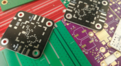
Structural electronics integrates electronic functionality directly into the physical structure of a product, eliminating the need for traditional circuit boards. This article examines how advances in materials, additive manufacturing, and flexible substrates are enabling compact, 3D, and wearable systems with enhanced performance and design freedom.
Blog
•
Beyond Traces: Why Soldermask May Be the Critical Factor in Ultra HDI
In ultra-HDI designs, soldermask is no longer a passive coating but a pivotal element that can determine manufacturability. This article explores why mask registration, resolution, and feature tolerances become critical as line spacings shrink below 50 µm.

Blog
•
How ECAD-MCAD Co-Design Supports Aerospace Reliability and Compliance
When the margin for error is nearly zero, aerospace engineering demands a design process that’s seamless across all domains. Here, we explore how ECAD-MCAD co-design delivers an integrated workflow that supports first-pass success and compliance with strict aerospace standards.

Blog
•
Most Common Causes of PCB Assembly Rework and Scrap
Many PCB assemblies fail not because of exotic faults, but due to basic issues like incorrect BOM entries or footprint mismatches that force rework or scrap. This article dives into the most common causes and how to prevent costly defects in your design-to-manufacturing process.

Blog
•
Behind the Scenes with AI Embedded Development
Forget one-shot AI hacks Ari Mahpour shows the thoughtful, sustainable way to integrate AI into embedded firmware development. Learn the core principles (planning gate, HAL abstraction, observability, timeout design) that can help you push your efficiency 5-10 times in real hardware projects.

Blog
•
We're heading to PCB West 2025!
Join Altium at PCB West 2025 in Santa Clara, CA, on October 1! Stop by Booth 300 for the official launch of the new Altium platform, built on the foundation of Altium Designer and Altium 365. Be sure to check out our live demos of Altium Develop and Altium Agile.

Blog
•
Peak Electrical Performance in Multi-Board Designs With Advanced Simulation and Compliance Tools
Moving from single-board to multi-board systems is a leap in complexity. You must manage not just routing, but power, signal integrity, mechanical fit, and regulatory requirements across boards. In this article, you’ll discover how Altium’s advanced simulation and compliance tools help engineering teams overcome these challenges and deliver reliable multi-board solutions.

Blog
•
How to Catch Enclosure and Connector Misalignment Before the First Prototype
As electronics continue to miniaturize and functionality increases, even minor misalignments between enclosures and connectors can derail a project. This article explores how early integration of ECAD and MCAD workflows helps detect and eliminate those costly issues before the first prototype is built.

Blog
•
Executive Insights Into Electronic Product Development Gaps You Need To Close
Electronics hardware development is falling behind broader product development disciplines due to fragmented workflows, poor collaboration, and limited compliance visibility. This gap introduces risk, delays, and missed opportunities but executives see real business value in modernizing electronics development through better integration, traceability, and lifecycle visibility.

Blog
•
Sourcing For High-Mix Low-Volume Electronics Manufacturing
High-mix, low-volume (HMLV) electronics manufacturing requires agile sourcing strategies to handle shifting BOMs, erratic lead times, and component volatility. All while controlling costs and ensuring compliance. Cloud-based tools like Altium provide real-time component visibility, BOM collaboration, and supplier integrations to help navigate HMLV complexities.










Your search returns no results.


