News & Updates

NEW

Blog
•
8 Common DFM Problems PCB Design Rules Catch Before Fab
Preventing DFM problems starts before fabrication not during the fab review. This article covers eight common PCB manufacturing issues and the design rules that help engineers identify and resolve them early.

NEW

Blog
•
What is a Multi-CAD Environment? Advantages and Best Practices
Different CAD tools shouldn't mean disconnected teams. Learn how Multi-CAD workflows help engineers review designs, collaborate across disciplines, and catch mechanical or sourcing issues before they become costly redesigns.

Blog
•
Deliver Production-Ready Multiboard PCBs Faster with Manufacturing-Driven Design
This article explores how manufacturing-driven design can help teams validate multiboard products before they reach the factory. It highlights how early checks of interconnects, harnesses, mechanical fit, sourcing, and manufacturing data can reduce late-stage changes and accelerate production readiness.


Blog
•
Stop Chasing Signatures: How Automated Design Sign-offs Accelerate Release Cycles
Automated design sign-offs can eliminate much of the administrative friction surrounding hardware approvals. This article explores how in-context reviews, structured workflows, and automated traceability help teams accelerate release cycles while maintaining control.


Blog
•
Flexible Circuits in Assembly: What PCB Designers Don’t See Until It’s Too Late
Flexible circuits introduce unique assembly challenges that aren't always visible during PCB design, from panel instability and component movement to thermal distortion during reflow. This article explains how design decisions around stiffeners, placement, panelization, and materials can improve assembly yield and reduce costly rework.


Blog
•
Requirements Management Lessons Learned: The S-80 Submarine Program
Fixing one design problem can sometimes create another you didn't see coming. This article uses the S-80 submarine program to show how better requirements traceability can help teams spot hidden impacts before they turn into expensive rework.

Blog
•
Trust Your BOM: Ensuring Design Data Integrity in Fast-Paced Hardware Projects
A BOM is only valuable if everyone can trust the data it contains. This article shows how connected BOM management helps teams eliminate errors, improve collaboration, and keep fast-moving hardware projects on schedule.

Blog
•
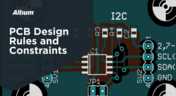
The Best PCB Design Rules System Keeps Your Board Error Free
PCB design rules are the foundation of every successful layout. This article explores how defining and managing constraints helps engineers improve design accuracy, simplify verification, and deliver manufacturing-ready PCBs with confidence.


Blog
•
Why Modern Electronics Teams Are Moving to a Cloud ECAD Platform
Great products are built by connected teams, not disconnected tools. This article shows how cloud ECAD platforms enable real-time co-design, structured design reviews, and seamless collaboration across engineering, manufacturing, and supply chain teams.


Blog
•
10 Questions to Ask Your Fabricator Before Submitting a Rigid-Flex Design
A five-minute conversation with your fabricator could save weeks of redesign. Discover the ten questions that can improve manufacturability, boost yield, and help your rigid-flex project succeed on the first build.

Blog
•
How Engineering Project Management Tools Are Changing Engineering Teams’ Productivity
Engineering project management tools play a critical role in managing timelines, resources, and cross-disciplinary coordination. This article breaks down the most impactful systems for improving execution and team performance.

Blog
•
7 Ways to Catch Rules & Constraints Early – Checklist
Discover seven actionable ways to spot and fix rules and constraint issues before they derail your PCB project. Using Altium Designer Agile, these tips help you build more manufacturable and reliable boards with fewer iterations.

Blog
•
Do You Need an IPC-D-356 Netlist?
If your output package is Gerber-based, adding an IPC-D-356 netlist can dramatically improve how your design is reviewed and validated for production. Here’s when it matters, what it contains, and how to generate it quickly in Altium.

Blog
•
How Agile BOM Management Helps You Lock in Pricing Before Market Shifts
When engineering and procurement work from different BOM versions, delays and cost surprises follow. Learn how agile BOM management brings teams onto one connected BOM so they can respond fast, manage risk, and lock pricing early.

Blog
•
Flexible Circuits: Enhancing Performance with Shielding, Heat Dissipation, and Stiffeners
A flex circuit can look perfect on paper and still fail in the real world due to EMI, hot spots, or mechanical strain. This article breaks down how shielding, thermal planning, and stiffeners help deliver designs that stay reliable over time.

Blog
•
Avoid These Top 3 Power Distribution Failures in PCB Design
Power distribution issues can silently undermine your PCB’s reliability. This article uncovers the top three failure modes and shows how Power Analyzer by Keysight helps you catch them early in the design phase and how Altium Agile Teams turns those checks into structured team action.

Blog
•
From BOM to Requirements and Back: Building Sourcing Constraints Into Specs
When engineering and procurement remain disconnected, supply-chain problems will sneak up on you. This guide argues convincingly: embed sourcing constraints into your requirements from day one, and avoid costly rework down the line.

Blog
•
Understanding Power Integrity in PCB Design: Power Analyzer by Keysight Whitepaper
Power integrity is the backbone of reliable PCB design. This whitepaper explains how to analyze and optimize voltage drop, current density, and grounding directly within Altium Designer Agile using the Power Analyzer by Keysight.
Blog
•
How to Manage ECAD Libraries for Consistent PCB Layout Design
Strong hardware starts with strong libraries. Discover how disciplined ECAD-library management dramatically improves design consistency and accelerates every stage of your PCB workflow.

Blog
•
High Speed PCB Design Review: Signal Integrity Questions You Should Always Ask
As data rates increase, the risks hidden in your layout grow with them. This quick guide highlights the critical SI checkpoints that can save you from late-stage surprises and redesigns. If you design high-speed boards, you’ll want to read this before your next review.

Blog
•
Supplier Negotiation: Turn Market Data Into Your Best Negotiation Tool
Don’t walk into supplier talks blind. Use market data to benchmark quotes, check lead times and uncover alternate parts. This article shows how visibility can shift the balance and de-risk your BOM.

Blog
•
Via-in-Pad in Rigid-Flex Designs: When Space Is Tight, Details Matter
Designing rigid-flex boards is like solving a 3D puzzle of materials, bends and tight spaces, and via-in-pad might just be the piece you need. Dive into how and when to use via-in-pad in rigid-flex designs, and what to watch out for from fabrication to field reliability.
Blog
•
Wearable Electronics: Innovations, Challenges & Future Trends
This whitepaper examines how next-generation wearable electronics are evolving through advancements in flexible and rigid-flex design, smart materials, AI, energy innovations, and connectivity. Discover what’s required to transform early prototypes into scalable, reliable products across healthcare, sports, defense, fashion, and enterprise applications.

Blog
•
Streamlining Component Selection for Long Product Lifecycles
Electronic parts may now cycle from launch to end-of-life in just a few years, but many systems are expected to serve for 10–20+ years. Here’s how to build a component selection process that aligns engineering, procurement and design for longevity and stability.

Blog
•
Using ECAD Software to Track Part Availability During PCB Design
As component lead-times extend and obsolescence becomes a persistent threat, PCB projects demand more than schematic capture and layout tools alone. This article details how ECAD software with embedded supply-chain intelligence can: unify engineering and procurement teams; provide visibility into stock levels, lead times and alternates; and enable proactive risk mitigation within the design loop.

Blog
•
PCB Design Data Management Tips for Multi-Board Projects
In complex electronic systems, managing data from multiple printed circuit boards can quickly become a logistical challenge. This article outlines a structured workflow for handling both board-level and assembly-level design outputs, ensuring clarity and consistency across fabrication, assembly and product-level documentation.

















On-Demand Webinar
•
Juni 12, 2025
Proactive Lifecycle Management: Preventing Obsolescence Before It Hits


On-Demand Webinar
•
Apr. 23, 2025
Collaborative Design Review: Ensuring Quality from Schematics to Supply Chain

On-Demand Webinar
•
Apr. 22, 2025
From Prototype to Production: Optimizing BOM Costs Without Compromising Quality with Part Analytics


On-Demand Webinar
•
Apr. 9, 2025
Component Selection in Altium Designer: Making Data-Driven Decisions with Data Integrations

On-Demand Webinar
•
März 25, 2025
Unlocking the full potential of your design team with Altium's enterprise solution



On-Demand Webinar
•
Jan. 24, 2024
Discover How Altium Designer 24 Revolutionizes Team Dynamics in PCB Design


