News & Updates
NEW
Blog
•
PCB Design Variants: Managing Multiple PCBA Versions
Product variations often require different component populations, alternate parts, or configuration settings while keeping the underlying PCB design unchanged. This article explains how structured variant management keeps these differences organized and ensures each configuration has the correct BOM and manufacturing outputs.

NEW
Blog
•
8 Common DFM Problems PCB Design Rules Catch Before Fab
Preventing DFM problems starts before fabrication not during the fab review. This article covers eight common PCB manufacturing issues and the design rules that help engineers identify and resolve them early.


Blog
•
What is a Multi-CAD Environment? Advantages and Best Practices
Different CAD tools shouldn't mean disconnected teams. Learn how Multi-CAD workflows help engineers review designs, collaborate across disciplines, and catch mechanical or sourcing issues before they become costly redesigns.

Blog
•
Deliver Production-Ready Multiboard PCBs Faster with Manufacturing-Driven Design
This article explores how manufacturing-driven design can help teams validate multiboard products before they reach the factory. It highlights how early checks of interconnects, harnesses, mechanical fit, sourcing, and manufacturing data can reduce late-stage changes and accelerate production readiness.


Blog
•
Stop Chasing Signatures: How Automated Design Sign-offs Accelerate Release Cycles
Automated design sign-offs can eliminate much of the administrative friction surrounding hardware approvals. This article explores how in-context reviews, structured workflows, and automated traceability help teams accelerate release cycles while maintaining control.

Blog
•
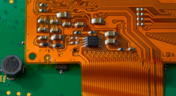
Flexible Circuits in Assembly: What PCB Designers Don’t See Until It’s Too Late
Flexible circuits introduce unique assembly challenges that aren't always visible during PCB design, from panel instability and component movement to thermal distortion during reflow. This article explains how design decisions around stiffeners, placement, panelization, and materials can improve assembly yield and reduce costly rework.


Blog
•
Requirements Management Lessons Learned: The S-80 Submarine Program
Fixing one design problem can sometimes create another you didn't see coming. This article uses the S-80 submarine program to show how better requirements traceability can help teams spot hidden impacts before they turn into expensive rework.

Blog
•
Trust Your BOM: Ensuring Design Data Integrity in Fast-Paced Hardware Projects
A BOM is only valuable if everyone can trust the data it contains. This article shows how connected BOM management helps teams eliminate errors, improve collaboration, and keep fast-moving hardware projects on schedule.

Blog
•
The Best PCB Design Rules System Keeps Your Board Error Free
PCB design rules are the foundation of every successful layout. This article explores how defining and managing constraints helps engineers improve design accuracy, simplify verification, and deliver manufacturing-ready PCBs with confidence.


Blog
•
Why Modern Electronics Teams Are Moving to a Cloud ECAD Platform
Great products are built by connected teams, not disconnected tools. This article shows how cloud ECAD platforms enable real-time co-design, structured design reviews, and seamless collaboration across engineering, manufacturing, and supply chain teams.


Blog
•
Mai 14, 2020
How to Highlight Nets in Altium Designer to Simplify Schematic and PCB Designs
Highlighting nets will help you simplify your schematic and PCB design. In Altium , there are multiple options that enable you to leverage this capability to simplify the verification of connections and circuit paths and make sure that the design you send to your manufacturer accurately reflects the printed circuit board you need built.

Blog
•
Mai 12, 2020
Keep Your Altium Designer PCB Layout in Line with Grids and Grid-Selection Shortcuts
The grid system in a printed circuit board design CAD system really is your friend, and if you haven’t taken the time to get properly introduced yet let me help you with that.

Blog
•
Mai 7, 2020
How to Panelize Your PCBs Before Lunch with Altium Designer
Whether you have a slew of PCBs to mass produce for your customers or a handful of project boards you wish to prototype all in one simple swoop, panelization is an effective way to bring high amounts of efficiency to your production.
Blog
•
Mai 5, 2020
Helpful Tips for Interactive Routing in Altium Designer
Before you jump into the software, you should know the types of things you’re going to want to look out for. Traces, connection lines, differential pair routing, and route paths can all affect the routing process of your board. Make sure that you’re equipped knowing, ultimately, what you want your board design to accomplish and furthermore, where you anticipate potential problem areas to be.

Blog
•
Mai 1, 2020
Altium 365 + Altium Designer 20.1 Released Today - Work from Anywhere, Connect with Anyone
In our efforts to bring the best experience to the PCB design process, we are proud to announce the release of Altium Designer 20.1, Altium 365, and Altium NEXUS Client 3.1. This release enhances the design experience by bringing the convenience and benefits of the Altium 365 cloud platform to Altium Designer.
Blog
•
Apr. 27, 2020
Introduction to High Speed PCB Designing: How to Eliminate Crosstalk
Crosstalk on your PCB layout can be disastrous. If not corrected, crosstalk can cause your finished circuit board to either not work at all, or it may be plagued by intermittent problems. Let’s take a look at what crosstalk is and what you can do to prevent it.
Blog
•
Apr. 22, 2020
Any Angle Routing: When Should You Use It?
EDA tools have come a long way since the advent of personal computing. Now advanced routing features like auto-routers, interactive routing, length tuning, and pin-swapping are helping designers stay productive, especially as device and trace densities increase. Read full article in our blog:
Blog
•
März 20, 2020
A Message from Altium on COVID-19
We understand that many of you, like ourselves, have transitioned to working remotely. This process comes with its challenges and we would like to offer all and any help we can to minimize disruptions for your teams and business.
Blog
•
März 2, 2020
About Altium Designer Home Page
With the new Altium Designer Home page, we are aiming to help users stay up to date with the latest features and productivity tricks available in Altium Designer. Learn more about the Home page in this documentation article.

Blog
•
Febr. 25, 2020
Getting Connected: Altium’s User Community Forums
The Altium design environment is a complex and sophisticated set of software tools. Not surprisingly, becoming proficient with these tools will take some time, and you’ll need to practice every step of the design process from beginning to end. So what happens if you get stuck along the way?







On-Demand Webinar
•
Juni 12, 2025
Proactive Lifecycle Management: Preventing Obsolescence Before It Hits


On-Demand Webinar
•
Apr. 23, 2025
Collaborative Design Review: Ensuring Quality from Schematics to Supply Chain

On-Demand Webinar
•
Apr. 22, 2025
From Prototype to Production: Optimizing BOM Costs Without Compromising Quality with Part Analytics


On-Demand Webinar
•
Apr. 9, 2025
Component Selection in Altium Designer: Making Data-Driven Decisions with Data Integrations
On-Demand Webinar
•
März 25, 2025
Unlocking the full potential of your design team with Altium's enterprise solution

On-Demand Webinar
•
Jan. 24, 2024
Discover How Altium Designer 24 Revolutionizes Team Dynamics in PCB Design


