News & Updates
NEW

Blog
•
PCB Design Variants: Managing Multiple PCBA Versions
Product variations often require different component populations, alternate parts, or configuration settings while keeping the underlying PCB design unchanged. This article explains how structured variant management keeps these differences organized and ensures each configuration has the correct BOM and manufacturing outputs.

NEW

Blog
•
8 Common DFM Problems PCB Design Rules Catch Before Fab
Preventing DFM problems starts before fabrication not during the fab review. This article covers eight common PCB manufacturing issues and the design rules that help engineers identify and resolve them early.


Blog
•
What is a Multi-CAD Environment? Advantages and Best Practices
Different CAD tools shouldn't mean disconnected teams. Learn how Multi-CAD workflows help engineers review designs, collaborate across disciplines, and catch mechanical or sourcing issues before they become costly redesigns.

Blog
•
Deliver Production-Ready Multiboard PCBs Faster with Manufacturing-Driven Design
This article explores how manufacturing-driven design can help teams validate multiboard products before they reach the factory. It highlights how early checks of interconnects, harnesses, mechanical fit, sourcing, and manufacturing data can reduce late-stage changes and accelerate production readiness.


Blog
•
Stop Chasing Signatures: How Automated Design Sign-offs Accelerate Release Cycles
Automated design sign-offs can eliminate much of the administrative friction surrounding hardware approvals. This article explores how in-context reviews, structured workflows, and automated traceability help teams accelerate release cycles while maintaining control.


Blog
•
Flexible Circuits in Assembly: What PCB Designers Don’t See Until It’s Too Late
Flexible circuits introduce unique assembly challenges that aren't always visible during PCB design, from panel instability and component movement to thermal distortion during reflow. This article explains how design decisions around stiffeners, placement, panelization, and materials can improve assembly yield and reduce costly rework.


Blog
•
Requirements Management Lessons Learned: The S-80 Submarine Program
Fixing one design problem can sometimes create another you didn't see coming. This article uses the S-80 submarine program to show how better requirements traceability can help teams spot hidden impacts before they turn into expensive rework.

Blog
•
Trust Your BOM: Ensuring Design Data Integrity in Fast-Paced Hardware Projects
A BOM is only valuable if everyone can trust the data it contains. This article shows how connected BOM management helps teams eliminate errors, improve collaboration, and keep fast-moving hardware projects on schedule.

Blog
•
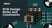
The Best PCB Design Rules System Keeps Your Board Error Free
PCB design rules are the foundation of every successful layout. This article explores how defining and managing constraints helps engineers improve design accuracy, simplify verification, and deliver manufacturing-ready PCBs with confidence.


Blog
•
Why Modern Electronics Teams Are Moving to a Cloud ECAD Platform
Great products are built by connected teams, not disconnected tools. This article shows how cloud ECAD platforms enable real-time co-design, structured design reviews, and seamless collaboration across engineering, manufacturing, and supply chain teams.


Blog
•
Wiring the Future: The Shift to Unified Electromechanical Design
This article explores the shift from PCB-centric design to complex, system-level development where wiring and harnesses play a critical role in product performance. It highlights how unified electromechanical workflows and bi-directional ECAD–MCAD integration improve accuracy, reduce delays, and ensure reliable, production-ready designs.
Blog
•
Best Tools For PCB DFM Checks
Want to catch manufacturability issues before they turn into expensive delays? Discover the essential DFM tools from real-time checks to post-layout analysis that help you get your PCB right the first time.

Blog
•
Eliminate Your Design Friction with Agile Teams
Design friction from scattered data and disconnected tools slows down PCB development and leads to rework. This webinar shows how Agile Teams streamlines collaboration, aligns domains, and helps teams deliver faster with fewer errors.

Blog
•
What Is an Integrated Design Environment for Electronics?
Using multiple disconnected tools slows down PCB development and increases the risk of errors. This article shows how an integrated environment keeps all design data connected, enabling faster workflows and fewer late-stage issues.

Blog
•
What is the Best Cloud PCB Design Software?
Not all cloud PCB tools are created equal, especially when design complexity increases. This article breaks down key differences between cloud-native and hybrid solutions, helping engineers choose the right approach for performance and scalability.

Blog
•
From Rework to Revenue: Digital PCB DFMA
This article explores how traditional, manual DFMA workflows lead to costly rework, delays, and poor collaboration across engineering teams. It shows how a connected, digital approach enables better data integrity, faster design cycles, and improved manufacturing outcomes.

Blog
•
Introducing Octopart Discover: From Part Search to Solutions Discovery
Octopart has announced Octopart Discover, a new platform that shifts electronic component search toward system-level solution discovery. The tool connects design intent with relevant options, enabling engineers to evaluate tradeoffs and identify the best-fit solutions more efficiently.

Blog
•
How to Choose the Right Components for Your BOM
A strong BOM can make the difference between smooth production and costly delays. Discover a practical approach to choosing components that stay available, meet compliance requirements, and keep your project on schedule.

Blog
•
From Scattered Requirements to Confident Product Development
See how the Requirements Portal transforms disconnected requirements into a single, live source of truth that engineers can trust at every stage of a project! Real customer stories in the article prove it’s already helping teams cut down on rework and bring products to market faster.

Blog
•
What is the Best PCB Design Tool For Students?
Students need PCB software that’s intuitive, affordable, and useful for building real skills. This article compares the strengths and weaknesses of leading design tools, from hobbyist platforms to industry-standard software.

Blog
•
What Is Collaborative Engineering?
Collaborative engineering is all about breaking down silos so electrical, mechanical, and sourcing teams can work as one with shared data and real-time updates. This article shows how that approach helps you spot issues early, reduce rework, and get products out the door with fewer surprises.

Blog
•
Bend Reliability: How Trace Geometry and Materials Impact Flex Lifespan
Focused on durability under repeated mechanical stress, this piece details how routing strategy, copper thickness, adhesive systems, and bend radius selection determine flex lifespan. Engineers will find actionable recommendations for reducing strain concentration and improving long-term performance in high-cycle applications.

Blog
•
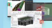
PCB Design Process: The EDA Design Approach
Dive into how a modern EDA workflow transforms PCB design by linking electrical, mechanical, and manufacturing requirements from idea to final release. With constraint‑driven integration, you can cut down on respins and bring better boards to market faster.
Blog
•
Getting Started for Mechanical Engineers
Explore our collection of MCAD Collaboration walkthroughs, where you’ll discover how to synchronize mechanical constraints and keepouts, maintain traceability with advanced history and revision control, and streamline electromechanical connectivity through harness synchronization. These topics and many more are covered in this article.

Blog
•
Are Your ECAD Tools Holding Back Engineers’ Productivity?
The article highlights that productivity issues often stem from tool limitations rather than engineer effort, especially as project complexity grows. ECAD tools that offer clear version control, cross-discipline integration, and workflow awareness are key to sustaining efficiency.

Blog
•
How Integrated PCB Design Cuts Development Time for Complex Electronics
Fewer tool handoffs, fewer errors, and smoother collaboration that’s the power of integrated PCB design. Learn how unifying your design environment can cut development time and help you deliver complex electronics faster.



On-Demand Webinar
•
Juni 12, 2025
Proactive Lifecycle Management: Preventing Obsolescence Before It Hits


On-Demand Webinar
•
Apr. 23, 2025
Collaborative Design Review: Ensuring Quality from Schematics to Supply Chain

On-Demand Webinar
•
Apr. 22, 2025
From Prototype to Production: Optimizing BOM Costs Without Compromising Quality with Part Analytics


On-Demand Webinar
•
Apr. 9, 2025
Component Selection in Altium Designer: Making Data-Driven Decisions with Data Integrations

On-Demand Webinar
•
März 25, 2025
Unlocking the full potential of your design team with Altium's enterprise solution


On-Demand Webinar
•
Jan. 24, 2024
Discover How Altium Designer 24 Revolutionizes Team Dynamics in PCB Design


