News & Updates
NEW

Blog
•
PCB Design Variants: Managing Multiple PCBA Versions
Product variations often require different component populations, alternate parts, or configuration settings while keeping the underlying PCB design unchanged. This article explains how structured variant management keeps these differences organized and ensures each configuration has the correct BOM and manufacturing outputs.

NEW

Blog
•
8 Common DFM Problems PCB Design Rules Catch Before Fab
Preventing DFM problems starts before fabrication not during the fab review. This article covers eight common PCB manufacturing issues and the design rules that help engineers identify and resolve them early.


Blog
•
What is a Multi-CAD Environment? Advantages and Best Practices
Different CAD tools shouldn't mean disconnected teams. Learn how Multi-CAD workflows help engineers review designs, collaborate across disciplines, and catch mechanical or sourcing issues before they become costly redesigns.

Blog
•
Deliver Production-Ready Multiboard PCBs Faster with Manufacturing-Driven Design
This article explores how manufacturing-driven design can help teams validate multiboard products before they reach the factory. It highlights how early checks of interconnects, harnesses, mechanical fit, sourcing, and manufacturing data can reduce late-stage changes and accelerate production readiness.


Blog
•
Stop Chasing Signatures: How Automated Design Sign-offs Accelerate Release Cycles
Automated design sign-offs can eliminate much of the administrative friction surrounding hardware approvals. This article explores how in-context reviews, structured workflows, and automated traceability help teams accelerate release cycles while maintaining control.

Blog
•
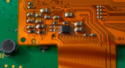
Flexible Circuits in Assembly: What PCB Designers Don’t See Until It’s Too Late
Flexible circuits introduce unique assembly challenges that aren't always visible during PCB design, from panel instability and component movement to thermal distortion during reflow. This article explains how design decisions around stiffeners, placement, panelization, and materials can improve assembly yield and reduce costly rework.


Blog
•
Requirements Management Lessons Learned: The S-80 Submarine Program
Fixing one design problem can sometimes create another you didn't see coming. This article uses the S-80 submarine program to show how better requirements traceability can help teams spot hidden impacts before they turn into expensive rework.


Blog
•
Trust Your BOM: Ensuring Design Data Integrity in Fast-Paced Hardware Projects
A BOM is only valuable if everyone can trust the data it contains. This article shows how connected BOM management helps teams eliminate errors, improve collaboration, and keep fast-moving hardware projects on schedule.

Blog
•
The Best PCB Design Rules System Keeps Your Board Error Free
PCB design rules are the foundation of every successful layout. This article explores how defining and managing constraints helps engineers improve design accuracy, simplify verification, and deliver manufacturing-ready PCBs with confidence.


Blog
•
Why Modern Electronics Teams Are Moving to a Cloud ECAD Platform
Great products are built by connected teams, not disconnected tools. This article shows how cloud ECAD platforms enable real-time co-design, structured design reviews, and seamless collaboration across engineering, manufacturing, and supply chain teams.


Blog
•
Why Use a Version Control System in PCB Design
Version Control Systems (VCS) have been around for many decades within the software world but can be surprisingly new to some folks in the electronics design industry. This article will cover what a VCS is, what it does, and why you should be using one for your PCB design projects.

Blog
•
Meeting Standards: IPC 6012 Class 3 Annular Ring
Designers often conflate leftover annular ring and pad sizes - they need to place a sufficiently large pad size on the surface layer to ensure that the annular ring that is leftover during fabrication will be large enough. As long as the annular ring is sufficiently large, the drill hit will not be considered defective and the board will have passed inspection. In this article, I'll discuss the limits on IPC-6012 Class 3 annular rings as these are a standard fabrication requirement for high-reliability rigid PCBs.

Blog
•
Decoding PCB Fabrication Notes
Sending a board out for fabrication is an exciting and nerve-wracking moment. Why not just give your fabricator your design files and let them figure it out? There are a few reasons for this, but it means the responsibility comes back to you as the designer to produce manufacturing files and documentation for your PCB. It’s actually quite simple if you have the right design tools. We’ll look at how you can do this inside your PCB layout and how this will help you quickly generate data for your manufacturer.

Blog
•
Design Basics for HDI and the HDI PCB Manufacturing Process
As the world of technology has evolved, so has the need to pack more capabilities into smaller packages. PCBs designed using high-density interconnect techniques tend to be smaller as more components are packed in a smaller space. An HDI PCB uses blind, buried, and micro vias, vias in pads, and very thin traces to pack more components into a smaller area. We’ll show you the design basics for HDI and how Altium Designer® can help you create a powerful HDI PCB.

Blog
•
Is It Printed or a Component? All About PCB Test Points
Test points in your electronic assembly will give you a location to access components and take important measurements to verify functionality. If you’ve never used a test point or you’re not sure if you need test points, keep reading to see what options you have for test point usage in your PCB layout.

Blog
•
How to Design to a Differential Impedance Specification
The concept and implementation of differential impedance are both sometimes misunderstood. In addition, the design of a channel to reach a specific differential impedance is often done in a haphazard way. The very concept of differential impedance is something of a mathematical construct that doesn’t fully capture the behavior of each signal in a differential trace. Keep reading to see a bit more depth on how to design to a differential impedance spec and exactly what it means for your design.

Blog
•
The Main Advantages when using Draftsman to Create a Component Mounting Drawing
Quite often, a standard assembly drawing is not enough to ensure the quality of a PCB assembly, especially when designing high-density boards. It would also be helpful to include additional detailing for simpler devices. The use of a Draftsman document brings an elegant, yet powerful solution to make these tasks easier.

Blog
•
Product Lifecycle Management in Electronics Manufacturing
An effective product lifecycle management (PLM) solution will integrate the tools and processes employed to design, develop and manufacture a new device. This solution goes beyond engineering activities to include the project management, process control, and financial management of the end-to-end business processes. PLM solutions create this collaborative environment where product development can flourish, bringing additional benefits in efficiencies and transparent communications, breaking silos, and speeding up the development process.

Blog
•
Should You Use Tight vs. Loose Differential Pair Spacing and Coupling?
In this article, we want to get closer to a realistic description of tight coupling vs. loose coupling in terms of differential pair spacing, as well as how the differential pair spacing affects things like impedance, differential-mode noise, reception of common-mode noise, and termination. As we’ll see, the focus on tight coupling has its merits, but it’s often cited as necessary for the wrong reasons.

Blog
•
How to Solve Your Engineering Design Review Challenges
You’ve possibly gone through plenty of engineering design reviews, both on the front-end of a project and the back-end before manufacturing. Engineering design reviews are performed to accomplish multiple objectives, and with many engineering teams taking a systems-based approach to design and production, electronics design teams will need to review much more than just a PCB layout and BOM. Today’s challenges with sourcing, manufacturability, reliability, and mechanical constraints are all areas that must be confronted in real designs

Blog
•
Schematic Review Checklist
One of the most common points of failure of a device occurs even before you start to layout your circuit board. Mistakes in your schematic design can easily make their way all the way into prototypes or production without a second thought once layout starts. In this article, I’m not going to extol the virtues of a good schematic design. Instead, this article is a simple no frills checklist.

Blog
•
PCB Via Current-Carrying Capacity: How Hot is Too Hot?
One common question from designers is current-carrying capacity of conductors in a PCB. Trace and via current-carrying capacity are legitimate design points to focus on when designing a new board that will carry high current. The goal is to keep conductor temperatures below some appropriate limit, which then helps keep components on the board cool. Let’s dig into the current state of thermal demands on vias in PCBs and how they compare to internal and external PCB traces.

Blog
•
Phalanx, not Failure: PCB Shielding to Protect Your Design
A combination of good printed circuit board design and good shielding mitigates EMI. Good PCB design for EMI shielding revolves around the layout, the placement of filters, and ground planes. A well-designed PCB minimizes parasitic capacitance and ground loops. Keep reading to learn more about PCB shielding.

Blog
•
Best Practices in Hardware Version Control Systems
Any project can get very complex, and the PCB design team needs to track revisions throughout a project. Why worry about tracking revisions? In the event you ever receive changes to product functional requirements, major changes are made to your product’s architecture, or you’re ready to finalize the design and prepare for fabrication, it’s best to clone a project at its current state and begin working on a new version. Keeping track of all these design changes in a PCB design project takes the type of hardware version control tools you’ll find in Altium 365™.

Blog
•
Copper Pour and Via Stitching: Do You Need Them in a PCB Layout?
To pour or not to pour, to stitch or not to stitch… Over many years, some common “rules of thumb” have become very popular and, ultimately, taken a bit out of context. Rules of thumb are not always wrong, but taking PCB design recommendations out of context helps justify bad design practices, and it can even affect the producibility of your board. Like many aspects of a physical PCB layout, via stitching and copper pour can be like acid: quite useful if implemented properly, but also dangerous if used indiscriminately.

Blog
•
Should You Use Power MOSFETs in Series?
Power MOSFETs enable a huge range of electronic systems, specifically in situations where BJTs are not useful or efficient. MOSFETs can be used in high current systems in parallel arrangements, but what about their use in series? Both arrangements of MOSFETs have their pitfalls that designers should consider. Let’s look at MOSFETs in series as they are quite useful in certain systems, but be careful to design your circuits and your PCB for reliability.



On-Demand Webinar
•
Juni 12, 2025
Proactive Lifecycle Management: Preventing Obsolescence Before It Hits


On-Demand Webinar
•
Apr. 23, 2025
Collaborative Design Review: Ensuring Quality from Schematics to Supply Chain

On-Demand Webinar
•
Apr. 22, 2025
From Prototype to Production: Optimizing BOM Costs Without Compromising Quality with Part Analytics



On-Demand Webinar
•
Apr. 9, 2025
Component Selection in Altium Designer: Making Data-Driven Decisions with Data Integrations

On-Demand Webinar
•
März 25, 2025
Unlocking the full potential of your design team with Altium's enterprise solution




On-Demand Webinar
•
Jan. 24, 2024
Discover How Altium Designer 24 Revolutionizes Team Dynamics in PCB Design


