News & Updates
NEW
Blog
•
PCB Design Variants: Managing Multiple PCBA Versions
Product variations often require different component populations, alternate parts, or configuration settings while keeping the underlying PCB design unchanged. This article explains how structured variant management keeps these differences organized and ensures each configuration has the correct BOM and manufacturing outputs.

NEW
Blog
•
8 Common DFM Problems PCB Design Rules Catch Before Fab
Preventing DFM problems starts before fabrication not during the fab review. This article covers eight common PCB manufacturing issues and the design rules that help engineers identify and resolve them early.


Blog
•
What is a Multi-CAD Environment? Advantages and Best Practices
Different CAD tools shouldn't mean disconnected teams. Learn how Multi-CAD workflows help engineers review designs, collaborate across disciplines, and catch mechanical or sourcing issues before they become costly redesigns.

Blog
•
Deliver Production-Ready Multiboard PCBs Faster with Manufacturing-Driven Design
This article explores how manufacturing-driven design can help teams validate multiboard products before they reach the factory. It highlights how early checks of interconnects, harnesses, mechanical fit, sourcing, and manufacturing data can reduce late-stage changes and accelerate production readiness.


Blog
•
Stop Chasing Signatures: How Automated Design Sign-offs Accelerate Release Cycles
Automated design sign-offs can eliminate much of the administrative friction surrounding hardware approvals. This article explores how in-context reviews, structured workflows, and automated traceability help teams accelerate release cycles while maintaining control.

Blog
•
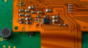
Flexible Circuits in Assembly: What PCB Designers Don’t See Until It’s Too Late
Flexible circuits introduce unique assembly challenges that aren't always visible during PCB design, from panel instability and component movement to thermal distortion during reflow. This article explains how design decisions around stiffeners, placement, panelization, and materials can improve assembly yield and reduce costly rework.


Blog
•
Requirements Management Lessons Learned: The S-80 Submarine Program
Fixing one design problem can sometimes create another you didn't see coming. This article uses the S-80 submarine program to show how better requirements traceability can help teams spot hidden impacts before they turn into expensive rework.

Blog
•
Trust Your BOM: Ensuring Design Data Integrity in Fast-Paced Hardware Projects
A BOM is only valuable if everyone can trust the data it contains. This article shows how connected BOM management helps teams eliminate errors, improve collaboration, and keep fast-moving hardware projects on schedule.

Blog
•
The Best PCB Design Rules System Keeps Your Board Error Free
PCB design rules are the foundation of every successful layout. This article explores how defining and managing constraints helps engineers improve design accuracy, simplify verification, and deliver manufacturing-ready PCBs with confidence.


Blog
•
Why Modern Electronics Teams Are Moving to a Cloud ECAD Platform
Great products are built by connected teams, not disconnected tools. This article shows how cloud ECAD platforms enable real-time co-design, structured design reviews, and seamless collaboration across engineering, manufacturing, and supply chain teams.


Blog
•
Simple Strategies to Reach 10% PCB Cost Reduction
Our new article outlines strategies to achieve a 10% reduction in PCB costs by optimizing design and material choices, such as adjusting stack-up materials and hole sizes, using lower-cost parts, and considering single-sided assembly. These techniques help reduce expenses without sacrificing quality.

Blog
•
Say Goodbye to EDA Software Vendor Lock
Check how Altium 365 helps eliminate EDA software vendor lock by enabling multi-CAD support in the cloud. This allows users to work with different CAD file formats within a single platform, enhancing collaboration and reducing the need for additional licenses. This approach offers greater flexibility and is set to transform the industry.

Blog
•
The Ultimate Introduction to High-Speed Signal Integrity for PCB Designers
High-speed signal integrity is essential in PCB design to ensure data accuracy and system reliability. Key issues like impedance mismatches, crosstalk, and signal reflections need to be addressed through strategies such as controlled impedance traces, differential pairs, and suitable material choices. Check out our first article of the series about this topic.
Blog
•
Multi-Board PCB Signal Integrity: A Complete Guide
Our new article on signal integrity in multi-board PCBs covers essential aspects like connector pinouts, cable designs, and interconnect strategies. These factors ensure reliable performance in high-speed applications across industries such as military, aerospace, and AI.
Blog
•
Multi-CAD Support Will Be a Game Changer for Electronics Design Teams
Discover how multi-CAD support is transforming electronics design with Altium 365 by enabling seamless integration of diverse CAD file formats. This innovation addresses vendor lock-in issues, boosting collaboration, version control, and project management across different CAD tools.
Blog
•
Pi.MX8 Project - Board Layout Part 4
We invite you to explore a new chapter in the PiMX8 Project, focusing on the final stages of PCB layout design for the Pi.MX8 compute module. This installment covers critical topics such as routing power planes and signal delay tuning, essential for ensuring proper functionality and performance.
Blog
•
How Thermoformed Flex PCB’s are Designed and Fabricated
Thermoformed flexible PCBs are specially designed and fabricated by heating and molding them into specific shapes, making them suitable for compact and complex applications like automotive dashboards and wearable devices. This process involves precise temperature control and careful handling to ensure durability and quality. Discover more from Tara Dunn's new article.
Blog
•
Boost Connection Integrity and Design Efficiency with Wire Bonding
Altium Designer's wire bonding feature enhances PCB design by supporting chip-up configurations for Chip on Board (CoB) designs. It offers easy validation of bond wiring in 3D views, ensuring accurate and efficient design processes. Check more about this feature on Altium's new feature page.
Blog
•
How High Frequency SMD Passives Work in a PCB Layout
High-frequency surface-mount device (SMD) passives like resistors and capacitors play a crucial role in PCB layouts, particularly in circuits operating above 1 GHz. Our article explores how these components function at high frequencies, their operational limits, and the importance of considering parasitic elements in design.

Blog
•
Essential DFM Tips for Aerospace Projects
Design for Manufacturing (DFM) is a crucial aspect of aerospace projects. This process ensures high-quality designs that meet the unique challenges of the aerospace industry, such as extreme conditions and stringent reliability standards. Learn more about essential DFM tips in our brand-new article.
Blog
•
Mechanics Meet Electronics Seamlessly in Multi-Board PCB Design
Curious about the intersection of mechanical and electrical design? Both are crucial in the PCB design process, especially for multi-board systems. Read our latest article to learn how ECAD and MCAD can address significant challenges during PCB preparation.

Blog
•
Altium 365 now has its own website!
Discover everything you need to know about Altium 365 and experience our suite of applications for secure, seamless, and streamlined collaboration. Visit now to explore how to streamline your electronic product development.
Blog
•
Efficient DC-DC Converter Design: Automated Measurements with Altium Designer 24 MixedSim
Automated measurements are no longer tough. With our Mixed Simulation mode, everything is easier. Learn more about this feature based on DC-DC buck converter design in this brand new article.
Blog
•
Altium Designer: Leading the Charge in PCB Design Innovation
In the dynamic field of electronics design, Altium Designer stands out as a pioneer, continuously advancing the boundaries of PCB (Printed Circuit Board) design. Discover the latest innovations in 3D-MID design, high-speed design, and interactive routing in this new article by David Marrakchi.
Blog
•
What Is Solder Mask Expansion and Which Value Should You Use?
Check out our new article explaining how to ensure sufficient pad area for soldering, manage misregistration tolerance, and maintain proper solder dams between components. It also highlights the role of collaboration with fabrication houses and the use of CAD tools in defining land patterns for advanced electronics designs.
Blog
•
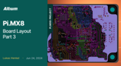
Pi.MX8 Project - Board Layout Part 3
We continue our exploration of the Pi.MX8 open-source computer module project. In this new installment, we focus on routing planning and then cover all the layers' routing with all the details you need to know if you want to prepare a similar project.



On-Demand Webinar
•
Juni 12, 2025
Proactive Lifecycle Management: Preventing Obsolescence Before It Hits


On-Demand Webinar
•
Apr. 23, 2025
Collaborative Design Review: Ensuring Quality from Schematics to Supply Chain

On-Demand Webinar
•
Apr. 22, 2025
From Prototype to Production: Optimizing BOM Costs Without Compromising Quality with Part Analytics


On-Demand Webinar
•
Apr. 9, 2025
Component Selection in Altium Designer: Making Data-Driven Decisions with Data Integrations
On-Demand Webinar
•
März 25, 2025
Unlocking the full potential of your design team with Altium's enterprise solution


On-Demand Webinar
•
Jan. 24, 2024
Discover How Altium Designer 24 Revolutionizes Team Dynamics in PCB Design


