News & Updates
Blog
•
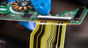
Bridging the Gap: When to Use Rigid-Flex Instead of Flex & Connector
Discover when a rigid-flex PCB is a better choice than a separate flex circuit and connector, especially for designs requiring compact packaging, repeated motion or high reliability. The article emphasizes that although rigid-flex needs more upfront planning and fabrication collaboration, it often pays off in simpler assemblies and improved performance.

Blog
•
Bridging Mechanical and Electrical Teams for Smarter Automotive Design
As vehicles evolve into advanced electronic systems, the separation between electrical and mechanical design teams becomes a critical bottleneck. This article explores how synchronized ECAD–MCAD workflows help automotive projects move faster, reduce rework and maintain design integrity.
Blog
•
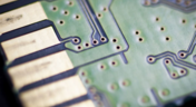
Via Structures: Designing for Reliability, Not Just Density
We all want to pack more into our PCB designs, but the smallest via isn’t always the smartest one. Dive in to learn how picking the right structure can save you headaches down the line.

Blog
•
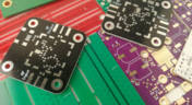
How Structural Electronics Enables 3D, Flexible, and Wearable Integration
Structural electronics integrates electronic functionality directly into the physical structure of a product, eliminating the need for traditional circuit boards. This article examines how advances in materials, additive manufacturing, and flexible substrates are enabling compact, 3D, and wearable systems with enhanced performance and design freedom.

Blog
•
Beyond Traces: Why Soldermask May Be the Critical Factor in Ultra HDI
In ultra-HDI designs, soldermask is no longer a passive coating but a pivotal element that can determine manufacturability. This article explores why mask registration, resolution, and feature tolerances become critical as line spacings shrink below 50 µm.

Blog
•
How ECAD-MCAD Co-Design Supports Aerospace Reliability and Compliance
When the margin for error is nearly zero, aerospace engineering demands a design process that’s seamless across all domains. Here, we explore how ECAD-MCAD co-design delivers an integrated workflow that supports first-pass success and compliance with strict aerospace standards.


Blog
•
Most Common Causes of PCB Assembly Rework and Scrap
Many PCB assemblies fail not because of exotic faults, but due to basic issues like incorrect BOM entries or footprint mismatches that force rework or scrap. This article dives into the most common causes and how to prevent costly defects in your design-to-manufacturing process.

Blog
•
Behind the Scenes with AI Embedded Development
Forget one-shot AI hacks Ari Mahpour shows the thoughtful, sustainable way to integrate AI into embedded firmware development. Learn the core principles (planning gate, HAL abstraction, observability, timeout design) that can help you push your efficiency 5-10 times in real hardware projects.

Blog
•
We're heading to PCB West 2025!
Join Altium at PCB West 2025 in Santa Clara, CA, on October 1! Stop by Booth 300 for the official launch of the new Altium platform, built on the foundation of Altium Designer and Altium 365. Be sure to check out our live demos of Altium Develop and Altium Agile.

Blog
•
Peak Electrical Performance in Multi-Board Designs With Advanced Simulation and Compliance Tools
Moving from single-board to multi-board systems is a leap in complexity. You must manage not just routing, but power, signal integrity, mechanical fit, and regulatory requirements across boards. In this article, you’ll discover how Altium’s advanced simulation and compliance tools help engineering teams overcome these challenges and deliver reliable multi-board solutions.

Blog
•
How to Catch Enclosure and Connector Misalignment Before the First Prototype
As electronics continue to miniaturize and functionality increases, even minor misalignments between enclosures and connectors can derail a project. This article explores how early integration of ECAD and MCAD workflows helps detect and eliminate those costly issues before the first prototype is built.

Blog
•
Is it Simultaneous Switching Noise or Crosstalk?
Going deeper into crosstalk, there is always the issue of verifying EMI/EMC compliance through test and measurement. With the multitude of signal integrity problems that can arise in real PCBs, how can the astute designer distinguish them all? Some problems are clearer than others, with specific signal integrity measurements being developed for testing and measuring particular aspects of signal behavior. The fact is, multiple signal integrity problems could be present on a single interconnect simultaneously.

Blog
•
Sharing PCB Data with Manufacturers in the Cloud
Once you’ve finished your new project and you’re ready to push it to your manufacturer, you’ll normally be stuck in an endless email chain with an engineer, or you’ll have to share cloud links with each other. The cloud sharing and design release tools in Altium Designer and Altium Concord Pro are a huge help in this area. In this post, I’m going to take an existing project I’ve worked with in a number of recent blogs, create some fabrication and assembly documentation, and finally push this data to a manufacturer using Altium Concord Pro.

Blog
•
The Great PCB Layout "Rules of Thumb" Debate Rages On
To this day, I still see many PCB layout “rules of thumb” that first became common nearly 20 years ago. Do these rules still universally apply? The answer is a firm “maybe.” The discussion around PCB layout rules of thumb is not that these rules are correct or incorrect. The problem is that the discussion around these rules often lacks context, leading to the always/never type of discussion seen in some popular forums. My goal in this article is to communicate the context behind the common PCB design rules.
Blog
•
How to Design Your PCB Test Coupon and What You Can Test
As the operating speed of components has increased, controlled impedance is becoming more common in digital, analog, and mixed-signal systems. If the controlled impedance value for an interconnect is incorrect, it can be very difficult to identify this problem during an in-circuit test. However, testing is normally performed on a PCB test coupon, which is manufactured on the same panel as the PCB. If you want to get through board spins quickly and aid future designs, you might consider designing a test coupon and keeping it handy for future designs.

Blog
•
Altium DbLibs and Electronic Components in the Cloud with Altium Designer 20.1
Altium’s DbLib support is one of the oldest and most loved features of Altium Designer for managing electronic components and their data. They’ve been present in the software world since before I could fathom the existence of Ohm’s law. Altium 20.1’s new Component Sync feature allows you to synchronize virtually any database or database Library with Altium 365, taking advantage of both approaches strengths.
Blog
•
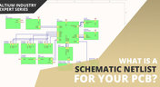
What is a Schematic Netlist for Your PCB?
If you’ve created your next great schematic, there is a lot going on behind the scenes in your design software. A schematic netlist is one of the central pieces of information that will be used in multiple features in your design software to create a real PCB. Your schematic netlist provides both electrical connectivity information, and reflects the functional structure of your design data in a single set of data.
Blog
•
How to Select an Inductor for a Buck Converter
An SMPS is one of those quiet (yet electrically noisy) devices that makes your favorite electronics run smoothly. Among the numerous DC-DC converter topologies, a buck converter finds plenty of uses for stepping down the input voltage to a lower level while providing high efficiency power conversion. A common question around component selection for these power converters is how to select an inductor for a buck converter. The goal in working with an inductor and other components in a buck converter is to limit power loss to heat and while minimizing current ripple.

Blog
•
US Department of Transportation Seeking Alternatives to GPS
GPS-capable devices range from your phone to your smartwatch; simply type in your destination and follow the directions. Simple, right? According to the Washington Post, we should all stop using GPS as it’s ruining the navigation centers of our brains. Despite the neurological effects on perception and judgment, the U.S. Department of Transportation (DOT) aims to find alternatives to GPS to provide redundancy.
Blog
•
Bluetooth 5.1 SoC vs. Module: Which is Best for Your Design?
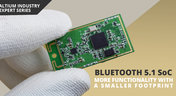
The list of features available in Bluetooth just got a little longer since the release of Bluetooth 5.1. If you want to incorporate a Bluetooth 5.1 SoC into your new product, you have two primary options for bringing this component into your board. The first is as an SoC that mounts to your board just like any other component. The other option is to bring a module into your new board—directly onto the surface layer. Here’s what you need to know about a Bluetooth 5.1 SoC or module in your next IoT product.

Blog
•
Altium 365 Getting Started User Guide - Available Now
Get Started with Altium 365 with a step-by-step guide and videos to experience the most connected experience for PCB design and realization: https://my.altium.com/altium-365/getting-started/

Blog
•
USB Power Delivery for Your Next Project
Since its introduction in the late 90s, the USB standard has never ceased to grow in popularity. There has been a growing trend toward USB being a power delivery interface with data, rather than a data interface that can supply power, as the 1.0 specification originally intended. To supply the increasing thirst for power over USB, the USB 3.0 Spec with Type-C began implementing the Power Delivery standard, which you should consider using for your next electronics project.
Blog
•
Circuit Board Design for In-Circuit Testing
There are many types of circuit board tests available in electronics manufacturing today, each having unique goals and characteristics. This article presents guidelines at the design level (schematic and layout) to enable the use of in-circuit testing (ICT) fixtures to verify proper component assembly. These simple test fixtures allow your board to be tested as its assembled, which helps identify and remove failed boards from your production run.

Blog
•
Planning for the Future with Cirris Systems and Altium
Technological advancements have been a hallmark of the past few decades, from the widespread adoption of internet technology to the smartphones and wireless devices we rely on every day to stay connected. Orlan Thatcher, Board Layout Specialist at Cirris Systems, could never have predicted the demand their services would generate. The company struggled with six different software platforms before switching to Altium Designer.

Blog
•
An Introduction to NFC
I used to work in a research lab that worked primarily with RFID (Radio Frequency IDentification) and NFC (Near Field Communication) technology, particularly for the agriculture industry and cattle identification. These were very specialized fields; however, the lab also worked on projects which involved retail and various other applications for NFC. It’s an amazing technology that you might be using every day without thinking about it - building access to your mobile phone payments, for instance.

Blog
•
Editing Your PCB Geometry with MCAD Tools
You need to define your PCB geometry in the context of your enclosure. If your board cannot physically be assembled into the final product, it doesn't matter how well laid out it is electrically. This webinar focuses on how the MCAD CoDesigner allows you to edit your PCB in the context of a higher-level assembly, allowing you to respect the relevant mechanical constraints.
Blog
•
The PCB Fabrication Process — what Every Design Engineer Needs To Know, Part 2
In Part 1 of this article, I described the first steps that occur during the PCB fabrication process. They detailed the inner layer processing effort as well as the efforts that take place during the transition from inner layer processing to lamination. This part of the article will provide a detailed description of the lamination, drilling and plating processes.
















Your search returns no results.


