News & Updates
Blog
•
Bridging the Gap: When to Use Rigid-Flex Instead of Flex & Connector
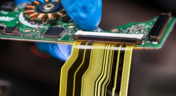
Discover when a rigid-flex PCB is a better choice than a separate flex circuit and connector, especially for designs requiring compact packaging, repeated motion or high reliability. The article emphasizes that although rigid-flex needs more upfront planning and fabrication collaboration, it often pays off in simpler assemblies and improved performance.

Blog
•
Bridging Mechanical and Electrical Teams for Smarter Automotive Design
As vehicles evolve into advanced electronic systems, the separation between electrical and mechanical design teams becomes a critical bottleneck. This article explores how synchronized ECAD–MCAD workflows help automotive projects move faster, reduce rework and maintain design integrity.
Blog
•
Via Structures: Designing for Reliability, Not Just Density
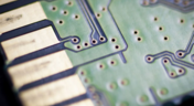
We all want to pack more into our PCB designs, but the smallest via isn’t always the smartest one. Dive in to learn how picking the right structure can save you headaches down the line.


Blog
•
How Structural Electronics Enables 3D, Flexible, and Wearable Integration
Structural electronics integrates electronic functionality directly into the physical structure of a product, eliminating the need for traditional circuit boards. This article examines how advances in materials, additive manufacturing, and flexible substrates are enabling compact, 3D, and wearable systems with enhanced performance and design freedom.

Blog
•
Beyond Traces: Why Soldermask May Be the Critical Factor in Ultra HDI
In ultra-HDI designs, soldermask is no longer a passive coating but a pivotal element that can determine manufacturability. This article explores why mask registration, resolution, and feature tolerances become critical as line spacings shrink below 50 µm.

Blog
•
How ECAD-MCAD Co-Design Supports Aerospace Reliability and Compliance
When the margin for error is nearly zero, aerospace engineering demands a design process that’s seamless across all domains. Here, we explore how ECAD-MCAD co-design delivers an integrated workflow that supports first-pass success and compliance with strict aerospace standards.


Blog
•
Most Common Causes of PCB Assembly Rework and Scrap
Many PCB assemblies fail not because of exotic faults, but due to basic issues like incorrect BOM entries or footprint mismatches that force rework or scrap. This article dives into the most common causes and how to prevent costly defects in your design-to-manufacturing process.


Blog
•
Behind the Scenes with AI Embedded Development
Forget one-shot AI hacks Ari Mahpour shows the thoughtful, sustainable way to integrate AI into embedded firmware development. Learn the core principles (planning gate, HAL abstraction, observability, timeout design) that can help you push your efficiency 5-10 times in real hardware projects.

Blog
•
We're heading to PCB West 2025!
Join Altium at PCB West 2025 in Santa Clara, CA, on October 1! Stop by Booth 300 for the official launch of the new Altium platform, built on the foundation of Altium Designer and Altium 365. Be sure to check out our live demos of Altium Develop and Altium Agile.
Blog
•
Peak Electrical Performance in Multi-Board Designs With Advanced Simulation and Compliance Tools
Moving from single-board to multi-board systems is a leap in complexity. You must manage not just routing, but power, signal integrity, mechanical fit, and regulatory requirements across boards. In this article, you’ll discover how Altium’s advanced simulation and compliance tools help engineering teams overcome these challenges and deliver reliable multi-board solutions.

Blog
•
How to Catch Enclosure and Connector Misalignment Before the First Prototype
As electronics continue to miniaturize and functionality increases, even minor misalignments between enclosures and connectors can derail a project. This article explores how early integration of ECAD and MCAD workflows helps detect and eliminate those costly issues before the first prototype is built.
Blog
•
How to Design a Microstrip to Waveguide Transition
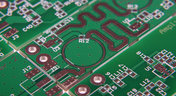
RF structures can be complicated to design and layout, particularly because many RF systems lead double lives as digital systems. Getting an analog signal out of a component and into a waveguide for high isolation routing is not so simple as placing a microstrip or stripline coming off your source component. Instead, you need to create a special microstrip to waveguide transition structure to ensure strong coupling into and out of your waveguide.

Blog
•
Managing PCB Polygon Pour and Copper Features in Complex Layouts
Layouts for complex electrical systems may need to make extensive use of copper pour to provide ground nets, power nets, shielding, and other copper structures for power and signal integrity. Backplanes, motherboards, RF products, and many other complex layouts will make use of copper pour and polygons that can’t be easily placed as custom components. The rules-driven design engine in Altium Designer® also ensures that any PCB polygon pour you place in your PCB layout will comply with clearance rules and will be checked against other electrical design rules.
Blog
•
High Speed Backplane Design and PCB Layout Tips
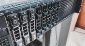
If you need to connect multiple boards into a larger system and provide interconnections between them, you’ll likely use a backplane to arrange these boards. Backplanes are advanced boards that borrow some elements from high speed design, mechanical design, high voltage/high current design, and even RF design. They carry their own set of standards that go beyond the reliability requirements in IPC.
Blog
•
PCIe 5.0 Signal Integrity and Analysis
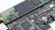
The upcoming Gen6 version of PCIe is pushing the limits of signal integrity for many computer systems designers. As with any high-speed signaling standard, signal integrity is a major design consideration, which requires the right set of design and analysis techniques. Rather than digging deep to find PCIe 5.0 signal integrity requirements from PCI-SIG, we’ve compiled the important points for today’s PCB layout engineers. Layout engineers should pay attention here as these design requirements will become more stringent in later PCIe generations.

Blog
•
Top 4 Time Wasters in PCB Design Collaboration
An essential aspect of project management is time management, especially when your design team is working remotely. Your time management strategy is team-based and individual, but time can easily get spent on important tasks when working as part of a team. So how can you streamline important collaboration tasks for your design team to increase productivity?

Blog
•
Sharing Inside and Outside Your Altium 365 Workspace
In these days of easily-available internet and quarantines, everyone is working remotely. It’s nice being able to spend time with family and regain control over your schedule, but keeping track of projects and revisions while securing user access feels like its own job. With the right set of project and data management tools, you can easily share your data with collaborators without tracking email chains.
Blog
•
How Your Altium 365 Workspace Keeps You Organized
When I started using my Altium 365 Workspace for collaboration, I found I could make things run more smoothly when I kept things organized. However, I prevented any issues thanks to all the organization tools built into the Explorer panel within Altium Designer. Let’s take a look at how you can get the most value out of your Altium 365 Workspace in terms of organization and access management.
Blog
•
How to Choose the Best PCB Manufacturer for Your Project
PCB manufacturing is competitive, and there is plenty of worldwide manufacturing capacity for new boards. If you’re looking for a manufacturer for your next project, it can be difficult to determine who is the best option to produce your board. Different fabricators and assemblers offer different levels of service, different capabilities, and access to different processes and materials. There are a lot of options to consider when selecting a manufacturer for your project.

Blog
•
Getting Started with Revision Control in Altium 365
Ever since I started using Github and Google Docs, I fell in love with revision control. Instead of keeping multiple copies of essential files and time-stamping every revision, revision tracking information gets stored alongside the file. This environment works great for code, spreadsheets, and documents, and Altium brings these same features into PCB design.

Blog
•
Image Processing Embedded Systems with Modular Hardware
With advances in industrial automation, automotive technology, remote sensing, and much more, image processing is taking center stage in many embedded systems. Image processing with older video systems was difficult or impossible due to the low quality of many imaging systems with perpetual uptime. Newer systems provide video with higher frame rates and higher resolution images, but these systems still needed to connect directly to a computer in order to enable any useful image processing applications.
Blog
•
Any Angle Routing: When Should You Use It?
EDA tools have come a long way since the advent of personal computing. Now advanced routing features like auto-routers, interactive routing, length tuning, and pin-swapping are helping designers stay productive, especially as device and trace densities increase. Routing is normally restricted to 45-degree or right-angle turns with typical layout and routing tools, but more advanced PCB design software allows users to route at any angle they like. So which routing style should you use, and what are the advantages of any angle routing?

Blog
•
Hardware-in-the-Loop Testing: An Introduction
If you do a search for “Hardware-in-the-Loop” testing, you will frequently find examples of complex, real-time systems. Article from National Instruments, for example, gives a nice explanation and background on what hardware-in-the-loop (HIL) is, and provides an example of testing electronic control units within an automobile. In this article, we will be focusing on a smaller, more bite-sized version of HIL testing concepts.

Blog
•
Near-field vs. Far-field EMI: What's Causing Noise Problems in My PCB?
If you’re an antenna designer, then you’re likely familiar with all aspects of near-field vs. far-field radiation. Given the litany of radiated EMI problems that cause noise within and outside of an electronic device, one might suddenly realize their new product is acting like a strong antenna. To understand how EMI affects your circuits, it helps to understand exactly how near-field vs. far-field radiation from your PCB affects your ability to pass EMC checks and affects your circuits.

Blog
•
Increasing PCB Prototype Iteration Speed in the Cloud
How often have you started down the PCB development process and been bogged down by time-consuming administrative tasks? Once you get ready for production, working through a design review and correcting any DFM problems takes its own share of time. With hastening product development timelines and shorter product life cycles comes the pressure to increase PCB prototype iteration speed without sacrificing cost or quality. So how can PCB design teams keep their development schedules on track without sacrificing quality or risking a failed prototyping run?

Blog
•
Why you should be using Concord Pro?
A journey of a thousand miles begins with a single step, or so the aphorism goes. I think it’s worth noting that the first step is the most difficult to take. Analysis Paralysis is especially true when dealing with a new software package, including the recent release of Concord Pro. The recent version has brought with it a deluge of interest and enthusiasm in such a phenomenal tool. But I must say, Altium hit this one out of the park.
Blog
•
What Types of EMI Filters are Best for Passing EMC Certification?
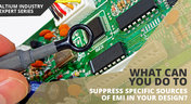
When you need to pass EMC certification and your new product is being crippled by a mysterious source of EMI, you’ll probably start considering a complete product redesign. Your stackup, trace geometry, and component arrangement are good places to start, but there might be more you can do to suppress specific sources of EMI. There are many different types of EMI filters that you can easily place in your design, and that will help suppress EMI in a variety of frequency ranges.







Your search returns no results.


