News & Updates
Blog
•
PCIe 5.0 Signal Integrity and Analysis
The upcoming Gen6 version of PCIe is pushing the limits of signal integrity for many computer systems designers. As with any high-speed signaling standard, signal integrity is a major design consideration, which requires the right set of design and analysis techniques. Rather than digging deep to find PCIe 5.0 signal integrity requirements from PCI-SIG, we’ve compiled the important points for today’s PCB layout engineers. Layout engineers should pay attention here as these design requirements will become more stringent in later PCIe generations.

Blog
•
Top 4 Time Wasters in PCB Design Collaboration
An essential aspect of project management is time management, especially when your design team is working remotely. Your time management strategy is team-based and individual, but time can easily get spent on important tasks when working as part of a team. So how can you streamline important collaboration tasks for your design team to increase productivity?


Blog
•
Sharing Inside and Outside Your Altium 365 Workspace
In these days of easily-available internet and quarantines, everyone is working remotely. It’s nice being able to spend time with family and regain control over your schedule, but keeping track of projects and revisions while securing user access feels like its own job. With the right set of project and data management tools, you can easily share your data with collaborators without tracking email chains.
Blog
•
How Your Altium 365 Workspace Keeps You Organized
When I started using my Altium 365 Workspace for collaboration, I found I could make things run more smoothly when I kept things organized. However, I prevented any issues thanks to all the organization tools built into the Explorer panel within Altium Designer. Let’s take a look at how you can get the most value out of your Altium 365 Workspace in terms of organization and access management.
Blog
•
How to Choose the Best PCB Manufacturer for Your Project
PCB manufacturing is competitive, and there is plenty of worldwide manufacturing capacity for new boards. If you’re looking for a manufacturer for your next project, it can be difficult to determine who is the best option to produce your board. Different fabricators and assemblers offer different levels of service, different capabilities, and access to different processes and materials. There are a lot of options to consider when selecting a manufacturer for your project.

Blog
•
Getting Started with Revision Control in Altium 365
Ever since I started using Github and Google Docs, I fell in love with revision control. Instead of keeping multiple copies of essential files and time-stamping every revision, revision tracking information gets stored alongside the file. This environment works great for code, spreadsheets, and documents, and Altium brings these same features into PCB design.

Blog
•
Image Processing Embedded Systems with Modular Hardware
With advances in industrial automation, automotive technology, remote sensing, and much more, image processing is taking center stage in many embedded systems. Image processing with older video systems was difficult or impossible due to the low quality of many imaging systems with perpetual uptime. Newer systems provide video with higher frame rates and higher resolution images, but these systems still needed to connect directly to a computer in order to enable any useful image processing applications.
Blog
•
Any Angle Routing: When Should You Use It?
EDA tools have come a long way since the advent of personal computing. Now advanced routing features like auto-routers, interactive routing, length tuning, and pin-swapping are helping designers stay productive, especially as device and trace densities increase. Routing is normally restricted to 45-degree or right-angle turns with typical layout and routing tools, but more advanced PCB design software allows users to route at any angle they like. So which routing style should you use, and what are the advantages of any angle routing?

Blog
•
Hardware-in-the-Loop Testing: An Introduction
If you do a search for “Hardware-in-the-Loop” testing, you will frequently find examples of complex, real-time systems. Article from National Instruments, for example, gives a nice explanation and background on what hardware-in-the-loop (HIL) is, and provides an example of testing electronic control units within an automobile. In this article, we will be focusing on a smaller, more bite-sized version of HIL testing concepts.

Blog
•
Near-field vs. Far-field EMI: What's Causing Noise Problems in My PCB?
If you’re an antenna designer, then you’re likely familiar with all aspects of near-field vs. far-field radiation. Given the litany of radiated EMI problems that cause noise within and outside of an electronic device, one might suddenly realize their new product is acting like a strong antenna. To understand how EMI affects your circuits, it helps to understand exactly how near-field vs. far-field radiation from your PCB affects your ability to pass EMC checks and affects your circuits.

Blog
•
Increasing PCB Prototype Iteration Speed in the Cloud
How often have you started down the PCB development process and been bogged down by time-consuming administrative tasks? Once you get ready for production, working through a design review and correcting any DFM problems takes its own share of time. With hastening product development timelines and shorter product life cycles comes the pressure to increase PCB prototype iteration speed without sacrificing cost or quality. So how can PCB design teams keep their development schedules on track without sacrificing quality or risking a failed prototyping run?

Blog
•
Why you should be using Concord Pro?
A journey of a thousand miles begins with a single step, or so the aphorism goes. I think it’s worth noting that the first step is the most difficult to take. Analysis Paralysis is especially true when dealing with a new software package, including the recent release of Concord Pro. The recent version has brought with it a deluge of interest and enthusiasm in such a phenomenal tool. But I must say, Altium hit this one out of the park.

Blog
•
What Types of EMI Filters are Best for Passing EMC Certification?
When you need to pass EMC certification and your new product is being crippled by a mysterious source of EMI, you’ll probably start considering a complete product redesign. Your stackup, trace geometry, and component arrangement are good places to start, but there might be more you can do to suppress specific sources of EMI. There are many different types of EMI filters that you can easily place in your design, and that will help suppress EMI in a variety of frequency ranges.
Blog
•
An Overview Of PCB Outer Layer Processing
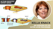
Previously, I described the PCB fabrication operations relative to inner layer processing, lamination, drilling, and plating. The last step in the process is outer layer processing which is described below. Once the desired plated copper thickness of a PCB has been achieved, it’s necessary to etch away the copper between the features in order to define the outer layer pattern.

Blog
•
How Do Pads and Vias Impact Total Capacitor Parasitic Inductance?
There are many factors at play in determining the impact of inductance on high-frequency power distribution systems. Two topic areas, inductance of the decoupling capacitor and inductance of the power planes, were addressed in earlier articles. This article will focus on the inductance of the capacitor footprint and via inductance from the capacitor footprint back to the PCB power planes.

Blog
•
Analyzing Crosstalk on FIFO and DDR4 Parallel Bus Interfaces
High-speed buses, whether single-ended or differential, can experience any number of signal integrity problems. A primary problem created by propagating signals is crosstalk, where a signal superimposes itself on a nearby trace. The industry-standard PCB design tools in Altium Designer® already include a post-layout simulator for examining crosstalk. Still, you can speed up crosstalk analysis in parallel buses when you use a powerful field solver.

Blog
•
Amplifier Stability at High Frequencies and Stray Capacitance
Any time-dependent physical system with feedback and gain has conditions under which the system will reach stable behavior. Amplifier stability extends these concepts to amplifiers, where the system output can grow to an undesired saturated state due to unintended feedback. If you use the right design and simulation tools, you can easily account for potential instability in your circuit models before you create your layout.

Blog
•
Low Cost Solutions for Automated Hardware in the Loop Testing
In today’s fast-paced world where iterations of electronics are spun at lightning speeds, we often forget one of the most critical aspects of development: testing. Even if we have that fancy test team, are we really able to utilize them for every modification, every small and insignificant change that we make to our prototypes? In this article, we will review a very low cost, yet highly effective and quite exhaustive test system that will get you that bang for your buck that you’ve been looking for.

Blog
•
Best Practices for Using DNI/DNP Entries in Your PCB BOM
If you’ve ever looked at the BOM for a reference design or an open-source project, you may have seen a comment in some of the entries in your BOM. This comment is either “DNP” or “DNI”. If you think about it, every component placed in the PCB requires some level of placement and routing effort, which takes time and money if you’re working for a client. This begs the question, why would anyone design a board with components they don’t plan to include in the final assembly?

Blog
•
Altium OutJob Files vs. Project Release: What's the Difference?
When it’s time to share your design data with your manufacturer, it’s like taking a leap of faith. Sending off a complete documentation package might seem as easy as placing your fab files in a zip folder, but there are better ways to ensure your manufacturer understands your project and has access to all your design data. For Altium Designer users, there are multiple options for creating and packaging release data into a complete package for your manufacturers.

Blog
•
Testing the Limits of Your LDO's Efficiency
If you’re designing a circuit board to be powered by anything except a bench-top regulated power supply, you’ll need to select a power regulator to place on your board. Just like any other component, your regulator has stated operating specs you’ll see in a product summary, and it has more detailed specs you’ll find in a datasheet. The fine details in your datasheets are easy to overlook, but they are the major factors that determine how your component will interact with the rest of your system.

Blog
•
How Total Harmonic Distortion Affects Your Power System
It would be nice if the power that came from the wall was truly noise-free. Unfortunately, this is not the case, and although a power system can appear to output a clean sine wave, zooming into an oscilloscope trace or using an FFT will tell you a different story. When you take "dirty" power, put it through rectification, and then pass it through a switching regulator, you introduce additional noise into the system that further degrades power quality. If you’re a power supply or power systems designer, then you know the value of supplying your devices with clean, noise-free power.

Blog
•
What PCB Copper Thickness Should You Use?
If you’re an electronics designer or you’re just beginning your career as an engineer, the PCB stackup is probably one of the last things you’ll think about. Simple items like PCB copper thickness and board thickness can get pushed to the back burner, but you’ll need to think about these two points for many applications as not every board will be fabricated on a standard 1.57 mm two-layer PCB

Blog
•
Should You Route Signals in Your PCB Power Plane?
I often get questions from designers asking about things like signal integrity and power integrity, and this most recent question forced me to think about some basic routing practices near planes and copper pour. "Is it okay to route signal traces on the same layer as power planes? I’ve seen some stackup guidelines that suggest this is fine, but no one provides solid advice." Once again, we have a great example of a long-standing design guideline without enough context.

Blog
•
The Anatomy of Your Schematic Netlist, Ports, and Net Names
Electronics schematics form the foundation of your design data, and the rest of your design documents will build off of your schematic. If you’ve ever worked through a design and made changes to the schematic, then you’re probably aware of the synchronization you need to maintain with the PCB layout. At the center of it all is an important set of data about your components: your schematic netlist. What’s important for designers is to know how the netlist defines connections between different components and schematics in a large project.

Blog
•
How to Compare PCB Manufacturing Services for Your Board
There are plenty of PCB manufacturing services you can find online, and they can all start to blend together. If you’re searching for a new service provider, it can be hard to compare all of them and find the best manufacturer that meets your needs. While experienced designers can spot bogus manufacturers from afar, there is always a temptation to go with the lowest priced, supposedly fastest overseas company you can find. However, there is a lot more that should go into choosing a PCB manufacturing service than just price.

Blog
•
Pi Filter Designs for Power Supplies
Pi Filters are a type of passive filter that gets its name from the arrangement of the three constituent components in the shape of the Greek letter Pi (π). Pi filters can be designed as either low pass or high pass filters, depending on the components used. The low-pass filter used for power supply filtering is formed from an inductor in series between the input and output with two capacitors, one across the input and the other across the output. Keep reading to learn more about their application in the PCB Design.
Blog
•
How to Design a Hybrid PCB Stackup
The first question that should come up when selecting materials and planning a stackup is: what materials are needed and how many layers should be used? Assuming you’ve determined you need a low-loss laminate and you’ve determined your required layer count, it’s time to consider whether you should use a hybrid stackup. There are a few broad situations where you could consider using a hybrid stackup with low-loss laminates in your PCB

Blog
•
Efficient Battery Power Supplies
Batteries offer a great power source for electrical devices that need to be mobile or located somewhere where connection to a mains electricity supply or other power source is impossible. The biggest problem with battery power is the expectation of users that the device will operate for significant periods with the need for recharging or replacing the batteries. This demand is placing the onus on the designer to improve efficiency and reduce power demand to meet this need.

Blog
•
What Target Impedance Should You Use in Your PDN?
A number of us on this blog and in other publications often bring up the concept of target impedance when discussing power integrity in high-speed designs. Some designs will be simple enough that you can take a “set it and forget it” approach to design a functional prototype. For more advanced designs, or if you’re fine-tuning a new board that has existing power integrity problems, target impedance is a real consideration that should be considered in your design.

Blog
•
An Overview of Dual Power Supply Design
Dual power supplies are circuits that generate two different output voltages from a single input source. The simplest method of generating dual output voltages is to use a transformer with two taps on the output winding. Bespoke transformers can have any voltage ratio depending on the number of windings in each part of the output side of the transformer.

Blog
•
Overlapping Planes in Your Mixed-Signal PCB Layout
With digital boards that are nominally running at DC, splitting up a power plane or using multiple power planes is a necessity for routing large currents at standard core/logic levels to digital components. Once you start mixing analog and digital sections into your power layers with multiple nets, it can be difficult to implement clean power in a design if you’re not careful with your layout.

Blog
•
Follow Mixed Signal PCB Design Guidelines With the Best CAD Tools
High-speed digital PCBs are challenging enough to design, but what about mixed-signal boards? Many modern systems contain elements that operate with both digital and analog signaling, and these systems must be designed to ensure signal integrity in both domains. Altium Designer has the layout and signal integrity tools you need to ensure your mixed-signal PCB design does not experience interference and obeys important design standards.











Your search returns no results.


