Welcome, Guest

Sign in to learn, create, and do more with the product you love.

News & Updates

Filters:
Tag
Embedded thumbnail for How to Work with The Polygon Manager
Working with Polygons
How to Work with The Polygon Manager

It is important to have a high-level view of all polygons on the PCB design. The Polygon Manager lets you rename polygons, set their pour order, perform re-pouring or disable pouring on selected polygons, add/scope the polygon connection style and clearance design rules, and add polygon classes for selected polygons.

PCB fabrication notes
Blog
Decoding PCB Fabrication Notes

Sending a board out for fabrication is an exciting and nerve-wracking moment. Why not just give your fabricator your design files and let them figure it out? There are a few reasons for this, but it means the responsibility comes back to you as the designer to produce manufacturing files and documentation for your PCB. It’s actually quite simple if you have the right design tools. We’ll look at how you can do this inside your PCB layout and how this will help you quickly generate data for your manufacturer.

Embedded thumbnail for Assigning Impedance Profiles for Differential Pairs
How to Work with Differential Pairs
Assigning Impedance Profiles for Differential Pairs

When you assign an impedance profile to a differential pair you open up several options for control over your routes. We'll show you how to do just that, as well as how to fix errors that may pop up and how to create classes for differential pairs based on assigned impedance profiles.

Embedded thumbnail for How to Highlight or Select Net Connections in the PCB
How-To's
How to Highlight or Select Net Connections in the PCB

We’ll show you how to highlight net selections so you can easily track where connections are made. We’ll show you how to hide and show nets, and how to use the view configuration and PCB panels to view and highlight nets across your design, and how to assign net colors in both the PCB and the schematic.

HDI PCB design and HDI PCB manufacturing process
Blog
Design Basics for HDI and the HDI PCB Manufacturing Process

As the world of technology has evolved, so has the need to pack more capabilities into smaller packages. PCBs designed using high-density interconnect techniques tend to be smaller as more components are packed in a smaller space. An HDI PCB uses blind, buried, and micro vias, vias in pads, and very thin traces to pack more components into a smaller area. We’ll show you the design basics for HDI and how Altium Designer® can help you create a powerful HDI PCB.

Embedded thumbnail for Remove Unused Via Pads
How to Design a BGA
Remove Unused Via Pads

The Remove Unused Pad Shapes tool in Altium Designer gives you control over the via pads in your design. We’ll show you how to use it to increase the usable area of power and ground polygons, increase the density of conductors between hole rows, and fixing incorrect connections.

All About PCB Test Points
Blog
Is It Printed or a Component? All About PCB Test Points

Test points in your electronic assembly will give you a location to access components and take important measurements to verify functionality. If you’ve never used a test point or you’re not sure if you need test points, keep reading to see what options you have for test point usage in your PCB layout.

Embedded thumbnail for Tent Vias under BGA
How to Design a BGA
Tent Vias under BGA

When via are located close to component pads some soldering issues can arise, but this can be fixed with Tented vias. We’ll show you how to manually tent vias and how to tent vias through the Design Rules.

How to Design to a Differential Impedance Specification
Blog
How to Design to a Differential Impedance Specification

The concept and implementation of differential impedance are both sometimes misunderstood. In addition, the design of a channel to reach a specific differential impedance is often done in a haphazard way. The very concept of differential impedance is something of a mathematical construct that doesn’t fully capture the behavior of each signal in a differential trace. Keep reading to see a bit more depth on how to design to a differential impedance spec and exactly what it means for your design.

Embedded thumbnail for Via-in-Pad for BGA
How to Design a BGA
Via-in-Pad for BGA

We’ll teach you how to use Via-in-pad to reduce inductance, improve signal integrity, and improve power distribution system performance in BGA designs.

Embedded thumbnail for Using HDI Stackups during BGA Design
How to Design a BGA
Using HDI Stackups during BGA Design

Micro Vias and Buried Vias play an important role in high density interconnection layer stackups (HDI Stackups). We’ll show you how to add via and create rules to allow you to take full advantage of the HDI Stackup.

Product Lifecycle Management in Electronics Manufacturing
Blog
Product Lifecycle Management in Electronics Manufacturing

An effective product lifecycle management (PLM) solution will integrate the tools and processes employed to design, develop and manufacture a new device. This solution goes beyond engineering activities to include the project management, process control, and financial management of the end-to-end business processes. PLM solutions create this collaborative environment where product development can flourish, bringing additional benefits in efficiencies and transparent communications, breaking silos, and speeding up the development process.

Article preview
On-Demand Webinar
Length Matching in High Speed Buses

With ever increasing speeds in high-speed data systems comes a couple of PCB layout challenges. High-speed busses like DDR, VME, PCIe just to mention a few can all reach data transfer speeds that require strict timing with very tight tolerances, thereby leaving very little slack in the PCB layout. Watch this on-demand webinar to learn why it's imperative to match track lengths in high-speed data systems and differential signals. You’ll see how to properly define PCB length matching and time delay constraints, and how to effectively route high-speed signals in Altium Designer®.

Tight versus loose coupling
Blog
Should You Use Tight vs. Loose Differential Pair Spacing and Coupling?

In this article, we want to get closer to a realistic description of tight coupling vs. loose coupling in terms of differential pair spacing, as well as how the differential pair spacing affects things like impedance, differential-mode noise, reception of common-mode noise, and termination. As we’ll see, the focus on tight coupling has its merits, but it’s often cited as necessary for the wrong reasons.

Embedded thumbnail for Automatic Fanout With BGA
How to Design a BGA
Automatic Fanout With BGA

When routing a BGA it can be necessary to use automatic fanout to make the routing process easier and faster. We’ll show you how to run the automatic fanout for routing a BGA and how the rules can affect the outcome of the route.

Embedded thumbnail for Specifying NSMD and SMD for BGA
How to Design a BGA
Specifying NSMD and SMD for BGA

BGA layouts use two types of pads: SMD, Solder Mask Pads, or NSMD, Non-Solder Mask Pads. Here we’ll walk you through the differences and how to specify and edit them for your layout.

Engineering Design Review Guide
Blog
How to Solve Your Engineering Design Review Challenges

You’ve possibly gone through plenty of engineering design reviews, both on the front-end of a project and the back-end before manufacturing. Engineering design reviews are performed to accomplish multiple objectives, and with many engineering teams taking a systems-based approach to design and production, electronics design teams will need to review much more than just a PCB layout and BOM. Today’s challenges with sourcing, manufacturability, reliability, and mechanical constraints are all areas that must be confronted in real designs

Embedded thumbnail for Via Shielding and Stitching
Via Stitching
Via Shielding and Stitching

Altium Designer gives you full control over your via shielding and stitching. We’ll show you how to use our shielding and stitching tools, how to alter their parameters, and how to remove any unwanted via shielding and stitching.

Schematic Review Checklist
Blog
Schematic Review Checklist

One of the most common points of failure of a device occurs even before you start to layout your circuit board. Mistakes in your schematic design can easily make their way all the way into prototypes or production without a second thought once layout starts. In this article, I’m not going to extol the virtues of a good schematic design. Instead, this article is a simple no frills checklist.

Tag
chip with neon illumination
Blog
How Does the Package PDN Impact Power Integrity?

Whenever we say something to the effect of “components can’t work without a correctly designed PCB,” we only have to look at component packaging for evidence. It is true that component packages come with parasitics that affect signal integrity, but there is one area that we don’t often look at in terms of component packaging: power integrity.
electrical circuit with microcontroller
Blog
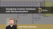
Designing Custom Hardware with Microcontrollers

In this article, we’ll look at all that is required to start creating your own custom microcontroller-based hardware designs. You’ll see that there actually isn’t too much to this, as microcontroller manufacturers over the years have tried to make the learning curve less steep and their devices more, and more accessible. This is both from an electrical point of view but also – equally importantly – from a programming point of view.


high-speed printed circuit board
Blog
Guide to Low-Dk PCB Materials

If you’ve taken time to learn about PCB material options and layer constructions, you have probably seen the wide range of materials that are available on the market. Materials companies produce laminates with varying Dk values, Tg values, weave styles, CTI values, and mechanical properties to target various applications in the electronics industry.

freeway in the background of the city
Blog
Designing for V2X Communication: Wireless Protocols and Standards

If you’re waiting for truly connected cars on a grand scale, there is still a massive amount of work to be done, both on the hardware and software sides. Connected cars can only become a widespread reality once the automotive industry and telecom carriers can decide which protocol will work best for vehicle-to-everything (V2X) communication. PCB designers will then need to step in to create these systems and fit them into a vehicular environment.

Everything You Need to Know About Stitching Vias
Blog
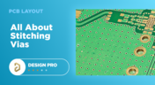
Everything You Need to Know About Stitching Vias

This one area of PCB design can be contentious among some designers as it is related to copper pour, which it is often stated is not needed in most designs. Regardless of your feelings about copper pour, stitching vias have important uses in PCBs at low frequencies and at high frequencies.

All About Box Build Assemblies
Blog
All About Box Build Assemblies

When you’re ready to manufacture a new device at production volume, there are many aspects of the product that must come together. The enclosure, cabling and connectors, embedded software/firmware, and of course the PCBA all have to be considered in totality. There is a quick way to get your product into a usable enclosure, complete with input power and cabling, and with a form factor that fits your PCBA. This overused route to a new product is a box build assembly. 

Ultra-HDI Technology is Not New
Blog
Ultra-HDI Technology is Not New

Printed circuit board fabricators have become skilled at manufacturing these technologies and also at understanding the reliability and producibility challenges associated with high-density-interconnect technology. Let’s look at where the PCB industry is at today. 

Today's PCB Designers Are Driving Electronics Product Design
Blog
Today's PCB Designers Are Driving Electronics Product Design

What can the industry do to support PCB designers as they continue taking a more active role in product development? Here at Altium, there has been a progressive shift towards looking at the system level and creating tools that get designers more involved throughout the product development process. As the saying goes, over the wall engineering is over… today’s most successful products are built in a collaborative process.

Phased Array Antenna Design for 5G Applications
Blog
Phased Array Antenna Design for 5G Applications

As the 5G rollout progresses and researchers continue to discuss 6G, many new 5G-capable products operating in sub-GHz and mmWave bands are reaching the marketplace. Devices that will include a 5G-compatible front-end, whether small stations/repeaters or handheld devices, use phased arrays as high-gain antenna systems to provide high data throughput without losing range at higher frequencies.

IPC - Vias
Blog
IPC - Vias

Via protection is an important part of modern PCB design. It provides additional benefits in PCB manufacturing and assembly, increasing the number of acceptable products.

Power Integrity Analysis in Your PCB Design Software
Blog
Power Integrity Analysis in Your PCB Design Software

Power integrity problems can abound in modern PCBs, especially high-speed boards that run with fast edge rates. These systems require precise design of the PDN impedance to ensure stable power is always delivered throughout the system.

Schematic Compare
Blog
Schematic Compare

A design project doesn’t appear out of nowhere. The design process spreads over time, and project documents change. Schematic documents gradually become more complex, new functional blocks appear, and already finished parts can be modified and updated.

Embedded Capacitance Materials Overview
Blog
Embedded Capacitance Materials Overview

Capacitance is your friend whenever you need stable power integrity, which is why there is so much focus on decoupling capacitors. While these components are important and they can be used to provide targeted power integrity solutions to certain components, there is one specialty material used to supercharge capacitance in your PCB stackup or package substrate. 

Tag
NEW
Embedded thumbnail for Future of Electronics Development in Security and Aerospace
How-To's
Future of Electronics Development in Security and Aerospace

See the highlights from Altium's executive event in Hamburg, where Security and Aerospace leaders explored AI-driven development, digital engineering, supply chain resilience, and the future of mission-critical electronics.

Embedded thumbnail for Create Clearance Rules Faster and with Less Effort
New in Altium's Software
Create Clearance Rules Faster and with Less Effort

Setting up clearance rules is now more intuitive in the Constraint Manager. Choose the Simple view for faster configuration with grouped object types, or the Advanced view when you need detailed, matrix-based clearance control.

Embedded thumbnail for Mastering HDI Design Rules in Altium Designer
How-To's
Mastering HDI Design Rules in Altium Designer

In our latest Altium Academy tutorial, we guide you through configuring the essential HDI PCB design rules in Altium's software. You'll learn how to use your manufacturer's fabrication capabilities to create accurate design rules and constraints for your PCB.

Embedded thumbnail for Search, Filter, and Navigate PCB Designs Faster
New in Altium's Software
Search, Filter, and Navigate PCB Designs Faster

The Web Viewer now features a redesigned search experience for faster access to PCB design data across supported CAD formats. A lightweight, intuitive interface lets you begin with simple search terms and progressively refine results using contextual suggestions.

Embedded thumbnail for Gain Better Control Over Wire Bond Visibility
New in Altium's Software
Gain Better Control Over Wire Bond Visibility

New bond wire visibility controls give you greater flexibility when working with wire-bonded boards and footprints, making it easier to focus on the details that matter most.

Embedded thumbnail for Coming Soon: Selectable Harness Source Within Multi-board Design
New in Altium's Software
Coming Soon: Selectable Harness Source Within Multi-board Design

Selectable Harness Source Within Multi-board Design enables harness projects to drive system connectivity while maintaining bidirectional synchronization between multi-board schematics and harness wiring diagrams for improved accuracy and easier design management.

Embedded thumbnail for Choose the Simbeor Version for Your PCB Calculations
New in Altium's Software
Choose the Simbeor Version for Your PCB Calculations

The PCB Editor now lets you choose the Simbeor version used for delay and impedance calculations, giving you more flexibility and consistency across your design workflows.

Embedded thumbnail for Improve PCB Editor Performance with Via Instancing
New in Altium's Software
Improve PCB Editor Performance with Via Instancing

The PCB Editor now uses via instancing to generate geometry for each via individually, providing greater flexibility and a more advanced approach to managing vias in PCB designs.

Embedded thumbnail for GSSG Stackup Deep Dive: Routing, Impedance, and HDI
How-To's
GSSG Stackup Deep Dive: Routing, Impedance, and HDI

A ground-signal-signal-ground (GSSG) stackup rethinks the traditional four-layer PCB structure by moving the ground planes to the outer layers and routing signals on the two inner layers. In this Altium Academy deep dive, we review a real one-minute design review submission and demonstrate how to configure a GSSG stackup properly using the Layer Stack Manager.

Embedded thumbnail for Generate IPC-7351B Compliant Footprints with More Control
New in Altium's Software
Generate IPC-7351B Compliant Footprints with More Control

The IPC Compliant Footprint Wizard has been updated to improve IPC-7351B compliance across supported package types. Enhancements include footprint calculations, package outlines, silkscreen and courtyard generation, layer mapping, density table behavior, and new pad trimming controls for gullwing packages, with support added to the batch generator Excel template.

Embedded thumbnail for Add Unit-Aware Temperature Coefficient Parameters
New in Altium's Software
Add Unit-Aware Temperature Coefficient Parameters

Component templates in a connected Workspace on the Altium Platform now include support for Temperature Coefficient (ppm/°C) as a unit-aware user parameter type. This makes it possible to define temperature coefficient values directly within the template using the appropriate units.

Embedded thumbnail for When to Add Part Numbers to SMD Passives
How-To's
When to Add Part Numbers to SMD Passives

Check out our new video covering essential electronics fundamentals, with a focus on why including part numbers for SMD passive components, such as SMD resistors, directly on schematics is so important. We also explore whether relying only on the Bill of Materials (BOM) is enough for effective electronic component management.

Embedded thumbnail for Present Large Harness Tables More Clearly
New in Altium's Software
Present Large Harness Tables More Clearly

Harness Draftsman now supports splitting connection tables across multiple pages in *.HarDwf documents. With the new page height limit setting, you can easily control how much of the table appears on each page.

Embedded thumbnail for Innovate Beyond - The Future of Electronics Development in Automotive
How-To's
Innovate Beyond - The Future of Electronics Development in Automotive

Discover how the future of automotive electronics is being shaped by a more connected development approach that unifies teams, data, requirements, design, collaboration, and manufacturing. Recorded at BMW Welt and the BMW Museum during Altium’s "The Future of Electronics Development in Automotive" event, this video explores the key challenges and innovations driving the next generation of automotive design.

Embedded thumbnail for Coming Soon: Design Rule Sets
New in Altium's Software
Coming Soon: Design Rule Sets

Soon, PCB design rules in Altium will be organized into reusable Rule Sets within the PCB Rules and Constraints Editor. These rule sets can be created, duplicated, enabled or disabled, renamed, deleted, imported, and exported, making it easier to manage rules for specific interfaces, manufacturing requirements, or unique design constraints.

Embedded thumbnail for Decoupling Capacitor Routing: When to Use Vias vs Traces
How-To's
Decoupling Capacitor Routing: When to Use Vias vs Traces

Check out this video, a follow-up to the decoupling capacitor placement series, exploring the inductance tradeoffs between trace routing and via connections. Using real component examples from an Ethernet switch design in Altium, the video demonstrates how different routing choices can impact overall performance.

Tag
Your search returns no results.