News & Updates


Blog
•
Copper Pour and Via Stitching: Do You Need Them in a PCB Layout?
To pour or not to pour, to stitch or not to stitch… Over many years, some common “rules of thumb” have become very popular and, ultimately, taken a bit out of context. Rules of thumb are not always wrong, but taking PCB design recommendations out of context helps justify bad design practices, and it can even affect the producibility of your board. Like many aspects of a physical PCB layout, via stitching and copper pour can be like acid: quite useful if implemented properly, but also dangerous if used indiscriminately.

Blog
•
Should You Use Power MOSFETs in Series?
Power MOSFETs enable a huge range of electronic systems, specifically in situations where BJTs are not useful or efficient. MOSFETs can be used in high current systems in parallel arrangements, but what about their use in series? Both arrangements of MOSFETs have their pitfalls that designers should consider. Let’s look at MOSFETs in series as they are quite useful in certain systems, but be careful to design your circuits and your PCB for reliability.


Blog
•
Controlled ESR Capacitors: Should You Use Them for Power Integrity?
I can’t think of a single product I’ve built that doesn’t require capacitors. We often talk a lot about effective series inductance (ESL) in capacitors and its effects on power integrity. What about effective series resistance (ESR)? Is there a technique you can use to determine the appropriate level of resistance, and can you use ESR to your advantage?


Blog
•
Microstrip Ground Clearance Part 2: How Clearance Affects Losses
If your goal is to hit a target impedance, and you’re worried about how nearby pour might affect impedance, you can get closer than the limits set by the 3W rule. But what are the effects on losses? If the reason for this question isn’t obvious, or if you’re not up-to-date on the finer points of transmission line design, then keep reading to see how nearby ground pour can affect losses in impedance-controlled interconnects.

Blog
•
Choosing the Right Microphone for Embedded Applications
If you need to capture sound waves for your electrical device to process, you'll need a microphone. However, microphones these days have become very advanced, and there are so many options to choose from. They range from the relatively simple and popular condenser type microphones to state-of-the-art sound conversion solutions incorporating internal amplifiers and other electronic processing functionality. In this article, we'll take a look at some of the options available.


Blog
•
Composite Amplifiers and How They Give the Best of Both Worlds
There are many times where you need an amplifier with high gain, low noise, high slew rate, and broad bandwidth simultaneously. However, not all of these design goals are possible with all off-the-shelf components. Here are some points to consider when working with a composite amplifier design and how to evaluate your design with the right set of circuit simulation tools.

Blog
•
Reduce Common-Mode Noise in Your Power Supply with Impedance Balancing
Simple switching regulator circuits that operate in compact spaces, like on a small PCB, can usually be deployed in noisy environments without superimposing significant noise on the output power level. As long as you lay out the board properly, you’ll probably only need a simple filter circuit to remove EMI on the inputs and outputs. As the regulator becomes larger, both physically and electrically, noise problems can become much more apparent, namely radiated EMI and conducted EMI in the PCB layout.


Blog
•
Part 1: Why Your PCB Design Review Process Is Obsolete and What You Can Do About It
A PCB design review is a practice to review the design of a board for possible errors and issues at various stages of product development. It can range from a formal checklist with official sign-offs to a more free-form inspection of schematic drawings and PCB layouts. For this article, we will not delve into what to check during a design review process but rather look at how a review process itself usually unfolds and how to optimize it to get the most out of your time.

Blog
•
Part 2: Why Your PCB Design Review Process Is Obsolete and What You Can Do About It
As we established in Part 1, the PCB design review and collaboration practices have room for improvement in many organizations. To address this, we developed Altium 365. Let's examine how running a PCB project through Altium 365 compares to other methods.


Blog
•
Efficiency And Noise Top 10 Switching Regulator Modules
Switching regulator modules have become indispensable in a wide array of electronic devices, providing a more efficient means of voltage conversion between different levels by storing and releasing energy. Explore further insights into these devices in today's dynamic world of electronics.
Blog
•
Add USB Type-C Power Delivery to Your Designs!
We want to invite you to explore the fundamentals of USB Type-C Power Delivery which is now the most popular energy transmission in current times. We will show you how to easily incorporate a dedicated PD IC into your own designs.
Blog
•
Design Phase – Lid Assembly Mechanics Part 1
It is time to delve deep into the mechanical design of our Open Source Laptop project. In this article we give you an update about the first part of fitting elements into the system. You will learn more about laptop lid, webcam integration, light sensor and microphones which will be used in this project.
Blog
•
How to Design for Test in Embedded Systems
Whether you're designing a high-speed PCB, or a complex embedded system, it will need some level of testing. In this article, we will show you some simple tricks that can make testing and debugging a prototype much easier.
Blog
•
Crosstalk Basics in PCB Design
Crosstalk is one of the most common issues related to electronics. Learn the basics of this phenomenon in PCB design, and gain knowledge on how to avoid it in your projects.
Blog
•
Top 3 Multi-Board PCB Connectivity Errors
Preparing complex PCB designs can often keep you awake at night. Learn more about some of the most common issues encountered in multi-board electrical connections.

Blog
•
Access to your Training Certificates on My Altium
Introduce an update on the My Altium user page that highlights your certificates and tracks your training progress, with one-click access to the Training Dashboard and Training Catalog pages. Easily view and share your certificates, keep an eye on your learning journey, and explore a variety of training resources.

Blog
•
Rigid-Flex PCBs: Advantages and Challenges
In this article, we will begin with a basic explanation of how rigid-flex technology differs from rigid board technology. We will then provide an overview of the advantages and conclude with a discussion of the challenges to be aware of.
Blog
•
When Should You Use Intrusive Soldering?
Through-hole components are frequently employed in power electronics, particularly when dealing with AC power from a wall outlet. In this article, you can delve into the intrusive soldering process and discover when it can be applied in PCB design.
Blog
•
Unveiling the Crucial Role of PCB Harness Design Capabilities in Multi-Board Designs
Multi-board designs are the key to meeting evolving demands, requiring robust PCB Harness Design for seamless interconnection and success. Join us as we explore the importance of PCB Harness Design capabilities and how they are crucial for the success of multi-board designs.
Blog
•
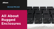
What Makes a PCB Enclosure Rugged?
Whether you purchase products off-the-shelf or online, they all come housed within an enclosure. In some cases, these enclosures are intentionally ruggedized to withstand harsh environments or mechanical shocks. You can learn more about enclosures in this new and interesting article.
Blog
•
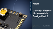
Concept Phase – Lid Assembly Design Part 2
We are continuing our journey through the lid assembly design phase of our Open Source Laptop project. In this section, we will discuss the layout of the test adapter and provide a demonstration of the first test for the display panel, along with the initial steps involved in assembling the boards.
Blog
•
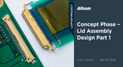
Concept Phase – Lid Assembly Design Part 1
In the exciting next phase of the open-source laptop project we're (finally) diving into design, and getting hands-on with the display panel. Discover how we're selecting the right panel, integrating it seamlessly, and creating a custom DisplayPort adapter to illuminate the screen. Plus, learn how our choices impact features like microphones, webcams, and touch sensors, and how Altium can help bring it all to life. It’s not too late to join as we continue on this innovative journey!
Blog
•
Unleashing the Power of Concurrent PCB Design
Concurrent PCB Design is essential to unlocking the full potential of engineering teams and delivering innovative products that meet the demands of the modern world. Learn more about the main capabilities and the numerous benefits of this upcoming feature in Altium Designer.

Blog
•
Crosstalk Reduction and Elimination Techniques in Altium Designer
Whether you're designing a digital board with a ton of traces, or an RF board operating at very high frequencies, any electronic device with propagating signals will experience crosstalk. Learn more about some sure-fire ways you can reduce crosstalk in your high-speed designs.

Blog
•
Baxandall Volume Control for Audio
The Baxandall volume control is an especially useful, flexible, and simple-to-implement circuit for numerous audio designs. In this article, we will demonstrate how to design this type of equipment.


Your search returns no results.


