News & Updates

Blog
•
When to Use Tented Vias in Your PCB Layout
There are some guidelines I see many designers implement as a standard practice, often without thinking about it. Some of these practices are misunderstood or implemented without best practices. Others are implemented without thinking about the potential problems. One of these is the use of tented vias, which is sometimes implemented in a PCB layout by default. Is this always the right practice?

Blog
•
How to Impedance Match and Terminate Capacitive Loads
The idea of a purely capacitive load is something of a fallacy. Yes, capacitors exist, but all capacitors are non-ideal, and it is this deviation from a theoretical capacitance that determines how to impedance match a load that exhibits capacitive behavior. Let’s take a look at this important aspect of interconnect design and see what it really means to terminate a capacitive load.

Blog
•
Using Altium 365 Over Your Vanilla Version Control System
There are all sorts of version control systems out there that people have been using with their PCB design software. As discussed in Why Use a Version Control System, we looked at different options ranging for local hard drive storage to sophisticated online revisioning systems. In this article we will be reviewing the differences between a standard VCS and Altium 365.
Blog
•
Why Use a Version Control System in PCB Design
Version Control Systems (VCS) have been around for many decades within the software world but can be surprisingly new to some folks in the electronics design industry. This article will cover what a VCS is, what it does, and why you should be using one for your PCB design projects.

Blog
•
Meeting Standards: IPC 6012 Class 3 Annular Ring
Designers often conflate leftover annular ring and pad sizes - they need to place a sufficiently large pad size on the surface layer to ensure that the annular ring that is leftover during fabrication will be large enough. As long as the annular ring is sufficiently large, the drill hit will not be considered defective and the board will have passed inspection. In this article, I'll discuss the limits on IPC-6012 Class 3 annular rings as these are a standard fabrication requirement for high-reliability rigid PCBs.

Blog
•
Decoding PCB Fabrication Notes
Sending a board out for fabrication is an exciting and nerve-wracking moment. Why not just give your fabricator your design files and let them figure it out? There are a few reasons for this, but it means the responsibility comes back to you as the designer to produce manufacturing files and documentation for your PCB. It’s actually quite simple if you have the right design tools. We’ll look at how you can do this inside your PCB layout and how this will help you quickly generate data for your manufacturer.



Blog
•
Design Basics for HDI and the HDI PCB Manufacturing Process
As the world of technology has evolved, so has the need to pack more capabilities into smaller packages. PCBs designed using high-density interconnect techniques tend to be smaller as more components are packed in a smaller space. An HDI PCB uses blind, buried, and micro vias, vias in pads, and very thin traces to pack more components into a smaller area. We’ll show you the design basics for HDI and how Altium Designer® can help you create a powerful HDI PCB.


Blog
•
Is It Printed or a Component? All About PCB Test Points
Test points in your electronic assembly will give you a location to access components and take important measurements to verify functionality. If you’ve never used a test point or you’re not sure if you need test points, keep reading to see what options you have for test point usage in your PCB layout.


Blog
•
How to Design to a Differential Impedance Specification
The concept and implementation of differential impedance are both sometimes misunderstood. In addition, the design of a channel to reach a specific differential impedance is often done in a haphazard way. The very concept of differential impedance is something of a mathematical construct that doesn’t fully capture the behavior of each signal in a differential trace. Keep reading to see a bit more depth on how to design to a differential impedance spec and exactly what it means for your design.

Blog
•
The Main Advantages when using Draftsman to Create a Component Mounting Drawing
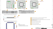
Quite often, a standard assembly drawing is not enough to ensure the quality of a PCB assembly, especially when designing high-density boards. It would also be helpful to include additional detailing for simpler devices. The use of a Draftsman document brings an elegant, yet powerful solution to make these tasks easier.


Blog
•
Product Lifecycle Management in Electronics Manufacturing
An effective product lifecycle management (PLM) solution will integrate the tools and processes employed to design, develop and manufacture a new device. This solution goes beyond engineering activities to include the project management, process control, and financial management of the end-to-end business processes. PLM solutions create this collaborative environment where product development can flourish, bringing additional benefits in efficiencies and transparent communications, breaking silos, and speeding up the development process.

Blog
•
Class-D Amplifier Design and PCB Layout
Amplifiers can come in all shapes and sizes, depending on their bandwidth, power consumption, and many other factors. A Class-D amplifier design is normally used with high fidelity audio systems, and circuits for a Class-D amplifier are not too difficult to build in a schematic. If you’ve never worked with a Class-D amplifier or you’re looking for a fun audio project, follow along with this PCB layout.

Blog
•
DDR5 vs. DDR6: Here's What to Expect in RAM Modules
Modern digital systems throw the digital electronics textbooks out the window, and high-speed DDR memories are a perfect example of the paradigm shift that occurs when you jump into IC and PCB design. With DDR5 still being finalized, and DDR6 now being discussed, designers who are already comfortable with DDR4 will need to consider how their design practices should adjust to accommodate the constant doubling of data speeds in these high-speed memory technologies.
Blog
•
Making the Most of Your Crystal Oscillator
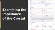
In my experience, the somewhat vague information you might find in a typical crystal datasheet doesn’t enable an engineer to be wholly confident that their design expectations can be met. On the other hand, “blindly” adopting what the crystal datasheet says usually results in adequate frequency stability. If you want to get inside and uncover what is going on, you need to start thinking about the crystal as a phase-shifting network.

Blog
•
How Antipads Affect Signal Integrity in Your Multilayer PCB
Antipads on vias and landing pads are a point of contention in modern PCB design, and the debate around the use of these elements in a multilayer PCB is framed as a binary choice. Like thermal reliefs, ground plane splits, and orthogonal routing, the debate around antipads on landing pads and vias is framed as an always/never choice. With today’s modern PCBs, it pays to understand the effects of antipads on signal integrity.
Blog
•
How to Design a Microstrip to Waveguide Transition
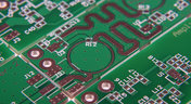
RF structures can be complicated to design and layout, particularly because many RF systems lead double lives as digital systems. Getting an analog signal out of a component and into a waveguide for high isolation routing is not so simple as placing a microstrip or stripline coming off your source component. Instead, you need to create a special microstrip to waveguide transition structure to ensure strong coupling into and out of your waveguide.

Blog
•
Managing PCB Polygon Pour and Copper Features in Complex Layouts
Layouts for complex electrical systems may need to make extensive use of copper pour to provide ground nets, power nets, shielding, and other copper structures for power and signal integrity. Backplanes, motherboards, RF products, and many other complex layouts will make use of copper pour and polygons that can’t be easily placed as custom components. The rules-driven design engine in Altium Designer® also ensures that any PCB polygon pour you place in your PCB layout will comply with clearance rules and will be checked against other electrical design rules.

Blog
•
High Speed Backplane Design and PCB Layout Tips
If you need to connect multiple boards into a larger system and provide interconnections between them, you’ll likely use a backplane to arrange these boards. Backplanes are advanced boards that borrow some elements from high speed design, mechanical design, high voltage/high current design, and even RF design. They carry their own set of standards that go beyond the reliability requirements in IPC.
Blog
•
PCIe 5.0 Signal Integrity and Analysis
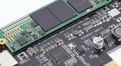
The upcoming Gen6 version of PCIe is pushing the limits of signal integrity for many computer systems designers. As with any high-speed signaling standard, signal integrity is a major design consideration, which requires the right set of design and analysis techniques. Rather than digging deep to find PCIe 5.0 signal integrity requirements from PCI-SIG, we’ve compiled the important points for today’s PCB layout engineers. Layout engineers should pay attention here as these design requirements will become more stringent in later PCIe generations.

Blog
•
Top 4 Time Wasters in PCB Design Collaboration
An essential aspect of project management is time management, especially when your design team is working remotely. Your time management strategy is team-based and individual, but time can easily get spent on important tasks when working as part of a team. So how can you streamline important collaboration tasks for your design team to increase productivity?

Blog
•
Sharing Inside and Outside Your Altium 365 Workspace
In these days of easily-available internet and quarantines, everyone is working remotely. It’s nice being able to spend time with family and regain control over your schedule, but keeping track of projects and revisions while securing user access feels like its own job. With the right set of project and data management tools, you can easily share your data with collaborators without tracking email chains.

Blog
•
How Your Altium 365 Workspace Keeps You Organized
When I started using my Altium 365 Workspace for collaboration, I found I could make things run more smoothly when I kept things organized. However, I prevented any issues thanks to all the organization tools built into the Explorer panel within Altium Designer. Let’s take a look at how you can get the most value out of your Altium 365 Workspace in terms of organization and access management.

Blog
•
How to Choose the Best PCB Manufacturer for Your Project
PCB manufacturing is competitive, and there is plenty of worldwide manufacturing capacity for new boards. If you’re looking for a manufacturer for your next project, it can be difficult to determine who is the best option to produce your board. Different fabricators and assemblers offer different levels of service, different capabilities, and access to different processes and materials. There are a lot of options to consider when selecting a manufacturer for your project.

Blog
•
Getting Started with Revision Control in Altium 365
Ever since I started using Github and Google Docs, I fell in love with revision control. Instead of keeping multiple copies of essential files and time-stamping every revision, revision tracking information gets stored alongside the file. This environment works great for code, spreadsheets, and documents, and Altium brings these same features into PCB design.

Blog
•
Image Processing Embedded Systems with Modular Hardware
With advances in industrial automation, automotive technology, remote sensing, and much more, image processing is taking center stage in many embedded systems. Image processing with older video systems was difficult or impossible due to the low quality of many imaging systems with perpetual uptime. Newer systems provide video with higher frame rates and higher resolution images, but these systems still needed to connect directly to a computer in order to enable any useful image processing applications.

Blog
•
Any Angle Routing: When Should You Use It?
EDA tools have come a long way since the advent of personal computing. Now advanced routing features like auto-routers, interactive routing, length tuning, and pin-swapping are helping designers stay productive, especially as device and trace densities increase. Routing is normally restricted to 45-degree or right-angle turns with typical layout and routing tools, but more advanced PCB design software allows users to route at any angle they like. So which routing style should you use, and what are the advantages of any angle routing?

Blog
•
Hardware-in-the-Loop Testing: An Introduction
If you do a search for “Hardware-in-the-Loop” testing, you will frequently find examples of complex, real-time systems. Article from National Instruments, for example, gives a nice explanation and background on what hardware-in-the-loop (HIL) is, and provides an example of testing electronic control units within an automobile. In this article, we will be focusing on a smaller, more bite-sized version of HIL testing concepts.
















Your search returns no results.


