News & Updates
Blog
•
When to Use Tented Vias in Your PCB Layout
There are some guidelines I see many designers implement as a standard practice, often without thinking about it. Some of these practices are misunderstood or implemented without best practices. Others are implemented without thinking about the potential problems. One of these is the use of tented vias, which is sometimes implemented in a PCB layout by default. Is this always the right practice?

Blog
•
How to Impedance Match and Terminate Capacitive Loads
The idea of a purely capacitive load is something of a fallacy. Yes, capacitors exist, but all capacitors are non-ideal, and it is this deviation from a theoretical capacitance that determines how to impedance match a load that exhibits capacitive behavior. Let’s take a look at this important aspect of interconnect design and see what it really means to terminate a capacitive load.

Blog
•
Using Altium 365 Over Your Vanilla Version Control System
There are all sorts of version control systems out there that people have been using with their PCB design software. As discussed in Why Use a Version Control System, we looked at different options ranging for local hard drive storage to sophisticated online revisioning systems. In this article we will be reviewing the differences between a standard VCS and Altium 365.
Blog
•
Why Use a Version Control System in PCB Design
Version Control Systems (VCS) have been around for many decades within the software world but can be surprisingly new to some folks in the electronics design industry. This article will cover what a VCS is, what it does, and why you should be using one for your PCB design projects.

Blog
•
Meeting Standards: IPC 6012 Class 3 Annular Ring
Designers often conflate leftover annular ring and pad sizes - they need to place a sufficiently large pad size on the surface layer to ensure that the annular ring that is leftover during fabrication will be large enough. As long as the annular ring is sufficiently large, the drill hit will not be considered defective and the board will have passed inspection. In this article, I'll discuss the limits on IPC-6012 Class 3 annular rings as these are a standard fabrication requirement for high-reliability rigid PCBs.

Blog
•
Decoding PCB Fabrication Notes
Sending a board out for fabrication is an exciting and nerve-wracking moment. Why not just give your fabricator your design files and let them figure it out? There are a few reasons for this, but it means the responsibility comes back to you as the designer to produce manufacturing files and documentation for your PCB. It’s actually quite simple if you have the right design tools. We’ll look at how you can do this inside your PCB layout and how this will help you quickly generate data for your manufacturer.



Blog
•
Design Basics for HDI and the HDI PCB Manufacturing Process
As the world of technology has evolved, so has the need to pack more capabilities into smaller packages. PCBs designed using high-density interconnect techniques tend to be smaller as more components are packed in a smaller space. An HDI PCB uses blind, buried, and micro vias, vias in pads, and very thin traces to pack more components into a smaller area. We’ll show you the design basics for HDI and how Altium Designer® can help you create a powerful HDI PCB.

Blog
•
Is It Printed or a Component? All About PCB Test Points
Test points in your electronic assembly will give you a location to access components and take important measurements to verify functionality. If you’ve never used a test point or you’re not sure if you need test points, keep reading to see what options you have for test point usage in your PCB layout.

Blog
•
How to Design to a Differential Impedance Specification
The concept and implementation of differential impedance are both sometimes misunderstood. In addition, the design of a channel to reach a specific differential impedance is often done in a haphazard way. The very concept of differential impedance is something of a mathematical construct that doesn’t fully capture the behavior of each signal in a differential trace. Keep reading to see a bit more depth on how to design to a differential impedance spec and exactly what it means for your design.

Blog
•
The Main Advantages when using Draftsman to Create a Component Mounting Drawing
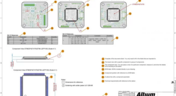
Quite often, a standard assembly drawing is not enough to ensure the quality of a PCB assembly, especially when designing high-density boards. It would also be helpful to include additional detailing for simpler devices. The use of a Draftsman document brings an elegant, yet powerful solution to make these tasks easier.


Blog
•
Product Lifecycle Management in Electronics Manufacturing
An effective product lifecycle management (PLM) solution will integrate the tools and processes employed to design, develop and manufacture a new device. This solution goes beyond engineering activities to include the project management, process control, and financial management of the end-to-end business processes. PLM solutions create this collaborative environment where product development can flourish, bringing additional benefits in efficiencies and transparent communications, breaking silos, and speeding up the development process.

Blog
•
Can You Fix a Warped PCB?
Before we get too deep into this article, I’ll give you the simple answer. You probably can’t fix warping in your PCB after it’s already been fabricated. You can prevent an unwarped board from becoming warped during assembly, but only as long as materials were selected properly and the board is put into reflow correctly. We’ll run over some of these points in this article, and I’ll examine some points that might help you recover a warped board.
Blog
•
What is an Eye Diagram?
The eye diagram is a useful measurement or simulation as part of channel compliance. The measurement shows many different factors that can affect signal behavior simultaneously, ultimately allowing for qualification of errors and losses in a channel. In this article, I’ll run over some of the fundamental measurements that you could manually extract from an eye diagram and how they reveal some strategies for improving channel designs.

Blog
•
What Skills Are Needed to be a PCB Layout Designer?
To readers who have been working in the PCB industry for most of your career, you have probably seen a very diverse group of professionals with varied skill sets and backgrounds. Designers might get started as engineers or as technicians, and some designers learn how to create beautiful PCB layouts in university. No matter how you got into PCB design, there are some important skills to know that will take you a long way towards advancing your career.
Blog
•
Beginner PCB Design Mistakes and How To Avoid Them
When starting out with PCB design, it’s common to treat the process as simply ‘connecting the dots’: as long as connections are made, it’s not particularly important how these connections are made. Having reviewed quite a number of PCBs of other PCB design engineers over the last few years, there are common, unfortunately erroneous, occurrences between a lot of them. This article aims to illustrate the top five beginner PCB design mistakes and what we can do to avoid making them. Let’s get started!

Blog
•
SAP (Semi-Additive PCB Process) – Top 5 Questions Regarding Stack Up
As the PCB design community embraces the benefits of this new printed circuit board fabrication technique, there are of course many questions to be answered. Today’s blog will address some of the most commonly asked questions related to circuit layer stack up as people are introduced to this new technology.
Blog
•
Altium Designer 22.9 Update
We are happy to announce that the Altium Designer 22.9 update is now available. Altium Designer 22.9 continues to focus on improving the user experience, as well as performance and stability of the software, based on feedback from our users. Check out the key new features in the What's New section on the left side of this window!
Blog
•
Dual Rail Voltage Supply
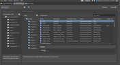
The highest performing operational amplifiers often need a split supply with positive and negative voltages connected to the op amps supply rails. In this project, we’re going to be building a positive/negative dual rail power supply for a differential oscilloscope probe I’m designing. I’m making the power supply a separate project, as a dual rail supply is quite useful to have, and I’m sure I’ll find multiple uses for it in the future.
Blog
•
Library Importer Improvements (former Library Migrator)
Importing file-based libraries from your local computer or network drive to your Altium 365 workspace can be done using the Library Importer. Altium’s Library Migrator was renamed Library Importer—the feature’s name was changed to conform more closely to the tool’s purpose. Not only is its name new, but our team has also made several user experience improvements. We have updated the documentation to reflect this change.

Blog
•
How to Select Copper Foil for High-Frequency PCB Design
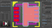
The PCB materials industry has spent significant amounts of time developing materials that provide lowest possible signal loss for products with RF applications. For high speed and high frequency designs, losses will limit signal propagation distance and distort signals, and it will create an impedance deviation that can be seen in TDR measurements. In this article, we'll look at the balance between copper foil losses and other types of losses in a PCB, as well as some strategies that are commonly used to overcome roughness.
Blog
•
Altium Designer 22.8 Update
We are happy to announce that the Altium Designer 22.8 update is now available. Altium Designer 22.8 continues to focus on improving the user experience, as well as performance and stability of the software, based on feedback from our users. Check out the key new features in the What's New section on the left side of this window!

Blog
•
What is Hybrid Beamforming?
In this article, we’ll look at beamforming implementation in an advanced method combining analog and digital techniques, known as hybrid beamforming. This method blends both digital and analog techniques to create multiple beams and thus reach multiple users with varying intensities. In the case of an RF imaging system or a radar system, hybrid beamforming in a MIMO technique also allows tracking of multiple targets with adjustable resolution.

Blog
•
Why Most Via Impedance Calculators Are Inaccurate
The problem with every via impedance calculator that I have seen is simple: they are incomplete or totally wrong. The “incomplete” part refers to a lack of context; these calculators can roughly reproduce a well-known estimate from a legend like Howard Johnson in his Digital Design textbooks. However, these calculators never provide insight into what they are actually calculating, or where the calculated via impedance is accurate. Keep reading to see why these calculators get it so wrong, as well as the context surrounding via impedance.

Blog
•
Buck Converter Simulation in Altium Designer
When designing high power circuits (usually very high voltage and/or current), you’ll need to create a regulator from scratch and place it in your PCB layout. It's also the case that you may want to model a real component using discretes in a simulation in order to qualify the system's expected operating regime. As part of buck converter design, you can easily run a buck converter simulation directly in Altium Designer’s schematic editor. Here’s how you can access these features in the newest version of Altium Designer.
Blog
•
Overview of the PCIe 6.0 Standard
Just as you get used to PCIe 5.0, they decide to release another standard! The newest iteration of PCIe is Gen6, or PCIe 6.0. PCIe 6.0 brings a doubling of channel bandwidth through introduction of PAM-4 as the signaling method in high-speed differential channels. This signaling method is a first for PCIe, and it’s an important enabler of the doubled data rate we see in the current standard. In this article, I’ll run over the important points in the standard and what PCB designers can expect when designing these channels.
Blog
•
SPI vs. I2C: How to Choose the Best Protocol for Your Memory Chips
One of the common implementations of SPI and I2C in a PCB layout is as a protocol for reading and writing to an external Flash memory. Flash chips are a very common component in embedded systems and can offer high capacities of non-volatile memory up to Gb values. When choosing a memory chip, you'll want to match the application requirements and functionality with the bus speed you need for read and write operations in your memory chip. There is also the matter of the type of Flash memory you'll need to access (NOR vs. NAND).
Blog
•
Is There an SPI Trace Impedance Requirement?
There is no SPI trace impedance requirement? The reality is that SPI lines only start to need impedance control when the length of the interconnect becomes very long. And because there is no specific impedance requirement in the bus, you have some freedom in channel design and termination. So what exactly qualifies as “very long” and when is some termination method needed? We’ll break it down in this article.















Your search returns no results.


