News & Updates
Blog
•
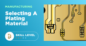
How to Choose PCB Plating for Your Finished Board
Once your board passes through the standard PCB fabrication process, the bare copper in your PCB will be ready for the application of a surface finish. PCB plating is applied to protect any copper in your PCB that would be exposed through the solder mask, whether it’s a pad, via, or other conductive element. In this article, I’ll run over the different PCB plating material options and their advantages in your PCB.



Blog
•
What is the PCB Supply Chain?
The PCB supply chain encompasses multiple components, raw materials, and the PCB itself. PCBs and PCB assemblies are often the most technically complex components that are purchased for electronic assemblies and products. The complexity of modern PCBs leads to several challenges for a supply chain management team that may be significantly different when compared with other commodities the team manages. In this brief guide, we'll look in-depth at the PCB supply chain, and specifically what falls within the purview of a procurement and supply chain management team.


Blog
•
A Guide to Mode Conversion, Its Causes, and Solutions
On interconnects, such as board-to-board connections or cascaded transmission line arrangements, you have an important EMC compliance metric that is sometimes overlooked. This is mode conversion, which can be visualized in an S-parameter measurement for differential and common-mode signal transmission. In this article, we’ll look at a short overview of mode conversion in high-speed design with some examples from common differential standards.


Blog
•
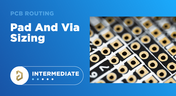
PCB Via Size and Pad Size Guidelines
There are some aspects of PCB design and layout that seem deceptively simple, and yet they have a complex answer that is related to many important aspects of manufacturing. One of these design aspects is the match between PCB via size and pad size. Obviously, these two points are related; all vias have a landing pad that supports the via and provides a place to route traces into a via pad. However, there are some important sizing guidelines to follow when the matching pad and via sizes, and this match is an important element of DFM and reliability.
Blog
•
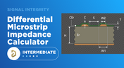
Differential Microstrip Impedance Calculator
Are you looking for a free tool that you can use to calculate the impedance of differential microstrips? We created a simple tool you can use to calculate differential microstrip impedance for a given geometry and dielectric constant. If you’ve been looking for an accurate differential microstrip impedance calculator, then the calculator below is certainly one of the best free tools you’ll find on the internet before you start using field solvers to determine differential pair impedance.


Blog
•
Getting Through a PCB DFM Check
In this article, we’ll discuss the key design features to implement, and steps to take prior to fabrication that will help prevent some common DFM problems. I’ll also provide examples of where I commonly see these PCB DFM problems in signal integrity circuits.


Blog
•
What is Spreading Inductance?
If you’re working with a high-speed digital component, there are some simple power integrity rules that should be followed. However, there is one quantity that is sometimes ignored when building a PDN impedance simulation: the spreading inductance of your plane pair. Here are some points designers should know about the spreading inductance of a plane pair.


Blog
•
PCB Design Basics for New Designers
In this article, I’ll present some design basics that every new designer should follow to help ensure their design process is successful. Some of these points may challenge the conventional view of how circuit boards are constructed, but they are intended to help balance low noise signaling, manufacturability, and ease of solving a layout.
Blog
•
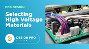
Selecting Materials for High Voltage PCB Design and Layout
High voltage PCBs are subject to certain safety and reliability concerns that you won’t find in most other boards. If your fabrication house specializes in high voltage PCBs and keeps materials in stock, they can likely recommend a material set, as well as a standard stackup you might use for certain voltage ranges and frequencies. If you need to choose your own materials, follow the tips below to help you narrow down to the right material set.


Blog
•
High-Speed Signal Routing: The 5 Important Constraints
After you capture your schematic as an initial layout and create an initial component arrangement, it’s time to define your routing constraints. Doing this early will allow your DRC engine to spot rules violations before you finish your layout. Likewise, you’ll be able to modify the default rule set to meet your layout requirements. Here are the important routing constraints you’ll need to check before you start routing your board.
Blog
•
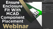
CoDesigner and MCAD Component Placement On-Demand Webinar
Learn how to place components from the MCAD side and synchronize them with Altium Designer ECAD models, designators, and sourcing data to simplify your design process.
Blog
•
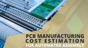
How to Create a PCB Manufacturing Cost Estimation
Some manufacturers have very convenient PCB manufacturing cost estimation calculators you can use, but the real costs depend on a number of factors. If you’re an entrepreneur and you’re producing your own boards, or you are managing manufacturing, testing, and delivery for a new project, it’s your job to help clients understand the primary cost drivers for new boards. Here’s how you can get an estimate of your fabrication costs, both for local and overseas manufacturers.
Blog
•
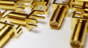
PCB Mountable Connectors: SMD vs. Through-hole
Selecting a connector is as much an art as it is a science. The artistic side is all about aesthetics and satisfying clearances, while the scientific side is all about signal integrity. For PCB mountable connectors, you’ll need to choose between surface-mounted or through-hole connectors, and you’ll need to consider how each type affects signal integrity in your application. Here’s what you need to think about beyond the standard connector specifications.

Blog
•
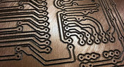
PCB Via Current-Carrying Capacity: How Hot is Too Hot?
Trace and via current-carrying capacity are legitimate design points to focus on when designing a new board that will carry high current. The goal is to keep conductor temperatures below some appropriate limit, which then helps keep components on the board cool.
Blog
•
How to Maximize Copper in Your PCB Design: The Pros and Cons of Copper Pouring Versus Placing
There is a saying in copper pour PCB design, “Copper is free.” It means a PCB editor designer must think in reverse. A board starts off as solid copper, and the copper you don’t want is removed. It is faster to build, less consumptive, and less expensive to make a board that is mostly copper as compared to the same size board that is mostly bare. Picking the correct technique will make the difference between an effortless or frustrating experience.

Blog
•
Top 5 PCB Design Guidelines Every PCB Designer Needs to Know
What’s the key to designing a board that’s realistic on paper and in physical form? Let’s explore the top 5 design guidelines that you need to know to design your next manufacturable, functional and reliable PCB.
Blog
•
5月 14, 2020
How to Highlight Nets in Altium Designer to Simplify Schematic and PCB Designs
Highlighting nets will help you simplify your schematic and PCB design. In Altium , there are multiple options that enable you to leverage this capability to simplify the verification of connections and circuit paths and make sure that the design you send to your manufacturer accurately reflects the printed circuit board you need built.

Blog
•
5月 12, 2020
Keep Your Altium Designer PCB Layout in Line with Grids and Grid-Selection Shortcuts
The grid system in a printed circuit board design CAD system really is your friend, and if you haven’t taken the time to get properly introduced yet let me help you with that.

Blog
•
5月 7, 2020
How to Panelize Your PCBs Before Lunch with Altium Designer
Whether you have a slew of PCBs to mass produce for your customers or a handful of project boards you wish to prototype all in one simple swoop, panelization is an effective way to bring high amounts of efficiency to your production.
Blog
•
5月 5, 2020
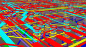
Helpful Tips for Interactive Routing in Altium Designer
Before you jump into the software, you should know the types of things you’re going to want to look out for. Traces, connection lines, differential pair routing, and route paths can all affect the routing process of your board. Make sure that you’re equipped knowing, ultimately, what you want your board design to accomplish and furthermore, where you anticipate potential problem areas to be.

Blog
•
5月 1, 2020
Altium 365 + Altium Designer 20.1 Released Today - Work from Anywhere, Connect with Anyone
In our efforts to bring the best experience to the PCB design process, we are proud to announce the release of Altium Designer 20.1, Altium 365, and Altium NEXUS Client 3.1. This release enhances the design experience by bringing the convenience and benefits of the Altium 365 cloud platform to Altium Designer.
Blog
•
4月 27, 2020
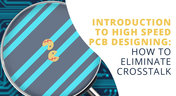
Introduction to High Speed PCB Designing: How to Eliminate Crosstalk
Crosstalk on your PCB layout can be disastrous. If not corrected, crosstalk can cause your finished circuit board to either not work at all, or it may be plagued by intermittent problems. Let’s take a look at what crosstalk is and what you can do to prevent it.
Blog
•
4月 22, 2020
Any Angle Routing: When Should You Use It?
EDA tools have come a long way since the advent of personal computing. Now advanced routing features like auto-routers, interactive routing, length tuning, and pin-swapping are helping designers stay productive, especially as device and trace densities increase. Read full article in our blog:
Blog
•
3月 20, 2020
A Message from Altium on COVID-19
We understand that many of you, like ourselves, have transitioned to working remotely. This process comes with its challenges and we would like to offer all and any help we can to minimize disruptions for your teams and business.
Blog
•
3月 2, 2020
About Altium Designer Home Page
With the new Altium Designer Home page, we are aiming to help users stay up to date with the latest features and productivity tricks available in Altium Designer. Learn more about the Home page in this documentation article.
















Your search returns no results.


