News & Updates


Blog
•
What is the PCB Supply Chain?
The PCB supply chain encompasses multiple components, raw materials, and the PCB itself. PCBs and PCB assemblies are often the most technically complex components that are purchased for electronic assemblies and products. The complexity of modern PCBs leads to several challenges for a supply chain management team that may be significantly different when compared with other commodities the team manages. In this brief guide, we'll look in-depth at the PCB supply chain, and specifically what falls within the purview of a procurement and supply chain management team.


Blog
•
A Guide to Mode Conversion, Its Causes, and Solutions
On interconnects, such as board-to-board connections or cascaded transmission line arrangements, you have an important EMC compliance metric that is sometimes overlooked. This is mode conversion, which can be visualized in an S-parameter measurement for differential and common-mode signal transmission. In this article, we’ll look at a short overview of mode conversion in high-speed design with some examples from common differential standards.



Blog
•
PCB Via Size and Pad Size Guidelines
There are some aspects of PCB design and layout that seem deceptively simple, and yet they have a complex answer that is related to many important aspects of manufacturing. One of these design aspects is the match between PCB via size and pad size. Obviously, these two points are related; all vias have a landing pad that supports the via and provides a place to route traces into a via pad. However, there are some important sizing guidelines to follow when the matching pad and via sizes, and this match is an important element of DFM and reliability.
Blog
•
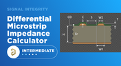
Differential Microstrip Impedance Calculator
Are you looking for a free tool that you can use to calculate the impedance of differential microstrips? We created a simple tool you can use to calculate differential microstrip impedance for a given geometry and dielectric constant. If you’ve been looking for an accurate differential microstrip impedance calculator, then the calculator below is certainly one of the best free tools you’ll find on the internet before you start using field solvers to determine differential pair impedance.



Blog
•
Getting Through a PCB DFM Check
In this article, we’ll discuss the key design features to implement, and steps to take prior to fabrication that will help prevent some common DFM problems. I’ll also provide examples of where I commonly see these PCB DFM problems in signal integrity circuits.


Blog
•
What is Spreading Inductance?
If you’re working with a high-speed digital component, there are some simple power integrity rules that should be followed. However, there is one quantity that is sometimes ignored when building a PDN impedance simulation: the spreading inductance of your plane pair. Here are some points designers should know about the spreading inductance of a plane pair.



Blog
•
PCB Design Basics for New Designers
In this article, I’ll present some design basics that every new designer should follow to help ensure their design process is successful. Some of these points may challenge the conventional view of how circuit boards are constructed, but they are intended to help balance low noise signaling, manufacturability, and ease of solving a layout.

Blog
•
Selecting Materials for High Voltage PCB Design and Layout
High voltage PCBs are subject to certain safety and reliability concerns that you won’t find in most other boards. If your fabrication house specializes in high voltage PCBs and keeps materials in stock, they can likely recommend a material set, as well as a standard stackup you might use for certain voltage ranges and frequencies. If you need to choose your own materials, follow the tips below to help you narrow down to the right material set.



Blog
•
When to Use Tented Vias in Your PCB Layout
There are some guidelines I see many designers implement as a standard practice, often without thinking about it. Some of these practices are misunderstood or implemented without best practices. Others are implemented without thinking about the potential problems. One of these is the use of tented vias, which is sometimes implemented in a PCB layout by default. Is this always the right practice?
NEW

Blog
•
Breaking the Multiboard Bottleneck: How Unified Design Solves ECAD–MCAD Disconnects
This article examines how fragmented ECAD-MCAD workflows create costly misalignments, late-stage conflicts, and inefficiencies in multiboard system design. It shows how unified, collaborative platforms enable real-time synchronization, digital twins, and cross-domain visibility to eliminate rework and streamline development.

Blog
•
Altium Designer vs. Flux For Professional PCB Projects
Choosing the right PCB tool can define your entire design workflow. Discover how Altium Designer empowers professional product development, while Flux.ai keeps things simple for fast experimentation.
Blog
•
Rigid-Flex Stackups: Where Good Designs Go Wrong Before Layout Even Starts
Rigid-flex stackups are more complex than they seem and getting them wrong early can lead to costly failures later. This article shows how smart decisions around materials, transitions, and layer structure help ensure a reliable design.

Blog
•
From Complexity to Clarity: Smart Design Reviews for Agile Engineering Teams
Understand how structured design reviews within Altium Agile Teams enhance visibility, traceability, and cross-team collaboration. This webinar highlights methods to detect issues early and optimize your development workflow.

Blog
•
Building a Local-LLM Datasheet Extractor for IC Driver Development
Parsing long datasheets manually slows down embedded development and introduces errors. This article shows how to use a local LLM pipeline to convert datasheets into structured data that speeds up driver creation.

Blog
•
Types of Simulation Tools For PCBs
PCB simulation isn’t one-size-fits-all and that’s where it gets interesting! Discover the wide range of tools available, from quick circuit checks to advanced multiphysics simulations, and how they help you design with confidence.

Blog
•
Wiring the Future: The Shift to Unified Electromechanical Design
This article explores the shift from PCB-centric design to complex, system-level development where wiring and harnesses play a critical role in product performance. It highlights how unified electromechanical workflows and bi-directional ECAD–MCAD integration improve accuracy, reduce delays, and ensure reliable, production-ready designs.
Blog
•
Best Tools For PCB DFM Checks
Want to catch manufacturability issues before they turn into expensive delays? Discover the essential DFM tools from real-time checks to post-layout analysis that help you get your PCB right the first time.

Blog
•
Eliminate Your Design Friction with Agile Teams
Design friction from scattered data and disconnected tools slows down PCB development and leads to rework. This webinar shows how Agile Teams streamlines collaboration, aligns domains, and helps teams deliver faster with fewer errors.

Blog
•
What Is an Integrated Design Environment for Electronics?
Using multiple disconnected tools slows down PCB development and increases the risk of errors. This article shows how an integrated environment keeps all design data connected, enabling faster workflows and fewer late-stage issues.

Blog
•
What is the Best Cloud PCB Design Software?
Not all cloud PCB tools are created equal, especially when design complexity increases. This article breaks down key differences between cloud-native and hybrid solutions, helping engineers choose the right approach for performance and scalability.

Blog
•
From Rework to Revenue: Digital PCB DFMA
This article explores how traditional, manual DFMA workflows lead to costly rework, delays, and poor collaboration across engineering teams. It shows how a connected, digital approach enables better data integrity, faster design cycles, and improved manufacturing outcomes.

Blog
•
Introducing Octopart Discover: From Part Search to Solutions Discovery
Octopart has announced Octopart Discover, a new platform that shifts electronic component search toward system-level solution discovery. The tool connects design intent with relevant options, enabling engineers to evaluate tradeoffs and identify the best-fit solutions more efficiently.

Blog
•
How to Choose the Right Components for Your BOM
A strong BOM can make the difference between smooth production and costly delays. Discover a practical approach to choosing components that stay available, meet compliance requirements, and keep your project on schedule.

Blog
•
From Scattered Requirements to Confident Product Development
See how the Requirements Portal transforms disconnected requirements into a single, live source of truth that engineers can trust at every stage of a project! Real customer stories in the article prove it’s already helping teams cut down on rework and bring products to market faster.

Blog
•
What is the Best PCB Design Tool For Students?
Students need PCB software that’s intuitive, affordable, and useful for building real skills. This article compares the strengths and weaknesses of leading design tools, from hobbyist platforms to industry-standard software.
















Your search returns no results.


