Welcome, Guest

Sign in to learn, create, and do more with the product you love.

News & Updates

Filters:
Tag
What is mode conversion
Blog
A Guide to Mode Conversion, Its Causes, and Solutions

On interconnects, such as board-to-board connections or cascaded transmission line arrangements, you have an important EMC compliance metric that is sometimes overlooked. This is mode conversion, which can be visualized in an S-parameter measurement for differential and common-mode signal transmission. In this article, we’ll look at a short overview of mode conversion in high-speed design with some examples from common differential standards.

Embedded thumbnail for Design RF PCB: routing (any angle, arc)
RF PCB Design
Design RF PCB: routing (any angle, arc)

It is worth taking a responsible approach to the shape and size of the RF signal conductors. In this video we will cover some practical aspects of working with routing such nets in Altium Designer.

Embedded thumbnail for Component Placement in Rigid-flex PCB
Working with MCAD CoDesigner extension
Component Placement in Rigid-flex PCB

With the MCAD CoDesigner you can quickly add and move components from your MCAD tool and update the design automatically in Altium Designer. We’ll show you how to add a new component, move components, change a component’s region in MCAD, and update your design in Altium Designer.

Pad and via sizing
Blog
PCB Via Size and Pad Size Guidelines

There are some aspects of PCB design and layout that seem deceptively simple, and yet they have a complex answer that is related to many important aspects of manufacturing. One of these design aspects is the match between PCB via size and pad size. Obviously, these two points are related; all vias have a landing pad that supports the via and provides a place to route traces into a via pad. However, there are some important sizing guidelines to follow when the matching pad and via sizes, and this match is an important element of DFM and reliability.

Differential Microstrip Impedance
Blog
Differential Microstrip Impedance Calculator

Are you looking for a free tool that you can use to calculate the impedance of differential microstrips? We created a simple tool you can use to calculate differential microstrip impedance for a given geometry and dielectric constant. If you’ve been looking for an accurate differential microstrip impedance calculator, then the calculator below is certainly one of the best free tools you’ll find on the internet before you start using field solvers to determine differential pair impedance.

Embedded thumbnail for Transmission lines (coplanar)
RF PCB Design
Transmission lines (coplanar)

The boards use transmission lines to carry high-frequency signals. In addition to microstrip lines, coplanar transmission lines with a ground reference polygon are often found on boards. Coplanar transmission lines propagate the same wave type as microstrip transmission lines, but the electromagnetic field is more concentrated near the conductor, so coplanar lines have lower losses at high frequencies, less dispersion, and less interference to adjacent circuits.

Embedded thumbnail for How to Reuse Board Shapes in MCAD
Working with MCAD CoDesigner extension
How to Reuse Board Shapes in MCAD

You can use the MCAD Co-designer panel to reuse your board shape or geometry in your PCB. We’ll show you how to use the MCAD Co-designer panel in Altium Designer and how to copy your board shape and geometry from your MCAD tool to Altium Designer.

PCB DFM Check
Blog
Getting Through a PCB DFM Check

In this article, we’ll discuss the key design features to implement, and steps to take prior to fabrication that will help prevent some common DFM problems. I’ll also provide examples of where I commonly see these PCB DFM problems in signal integrity circuits.

Embedded thumbnail for Selection filter - Panel Properties and PCB
How to work with Selection
Selection filter - Panel Properties and PCB

Learn how to configure the types of selected objects using the Selection Filter. In addition, you will learn about the Post Selection Filter and its features.

Spreading Inductance
Blog
What is Spreading Inductance?

If you’re working with a high-speed digital component, there are some simple power integrity rules that should be followed. However, there is one quantity that is sometimes ignored when building a PDN impedance simulation: the spreading inductance of your plane pair. Here are some points designers should know about the spreading inductance of a plane pair.

Embedded thumbnail for PCB Origins During the ECAD MCAD Exchange
Working with MCAD CoDesigner extension
PCB Origins During the ECAD MCAD Exchange

Origins can vary from your MCAD tool and Altium Designer. With the MCAD Co-Designer panel Altium Designer can keep track of your origin point and make sure your design changes are exchanged correctly.

Embedded thumbnail for Global Editing Using Find Similar Objects
How to work with Selection
Global Editing Using Find Similar Objects

Editing multiple objects one by one can be a very time consuming process. Altium Designer makes this easy and efficient with the Find Similar Objects tool, which allows you to globally select and edit multiple objects at once.

PCB Design Basics for New Designers
Blog
PCB Design Basics for New Designers

In this article, I’ll present some design basics that every new designer should follow to help ensure their design process is successful. Some of these points may challenge the conventional view of how circuit boards are constructed, but they are intended to help balance low noise signaling, manufacturability, and ease of solving a layout.

Selecting Materials for High Voltage PCB Design and Layout
Blog
Selecting Materials for High Voltage PCB Design and Layout

High voltage PCBs are subject to certain safety and reliability concerns that you won’t find in most other boards. If your fabrication house specializes in high voltage PCBs and keeps materials in stock, they can likely recommend a material set, as well as a standard stackup you might use for certain voltage ranges and frequencies. If you need to choose your own materials, follow the tips below to help you narrow down to the right material set.

Embedded thumbnail for Shaping the PCB in MCAD
Working with MCAD CoDesigner extension
Shaping the PCB in MCAD

Through the MCAD Co-designer in Altium Designer, you can collaborate with a mechanical engineer to shape the PCB in your MCAD tool and keep it updated in Altium Designer. We’ll show you how in Altium Designer and in your MCAD tool.

Embedded thumbnail for Cross Select Mode
How to work with Selection
Cross Select Mode

Cross Select Mode is a unique tool that allows for cross-selection of objects between the schematic and PCB thanks to the Altium Unified platform. This makes it easy to look for specific components, as well as take advantage of component placement tools.

Via tenting in PCB Layout
Blog
When to Use Tented Vias in Your PCB Layout

There are some guidelines I see many designers implement as a standard practice, often without thinking about it. Some of these practices are misunderstood or implemented without best practices. Others are implemented without thinking about the potential problems. One of these is the use of tented vias, which is sometimes implemented in a PCB layout by default. Is this always the right practice?

Embedded thumbnail for Tools for Efficient Selection
How to work with Selection
Tools for Efficient Selection

Efficient selection tools can make a difference in how long and how clean your design can be. Learn how to utilize the Edit Select Menu tools in Altium Designer to take control over your layout.

Capacitive load termination
Blog
How to Impedance Match and Terminate Capacitive Loads

The idea of a purely capacitive load is something of a fallacy. Yes, capacitors exist, but all capacitors are non-ideal, and it is this deviation from a theoretical capacitance that determines how to impedance match a load that exhibits capacitive behavior. Let’s take a look at this important aspect of interconnect design and see what it really means to terminate a capacitive load.


Embedded thumbnail for Tools for Easily Selecting Objects in the PCB
How to work with Selection
Tools for Easily Selecting Objects in the PCB

Explore more than basic mouse movements by taking a look at the tools that Altium Designer has to offer for making selecting and moving objects in the PCB an easy task. This will increase your productivity and allow you to spend more time designing

Tag
Benefits of Ultra HDI
Blog
The Benefits of Ultra HDI

Learn more about the combination of using both flexible materials and ultra-HDI feature sizes in this article.

Blog
Concept Phase – Cooling and Airflow Part 1

Next step in our open-source laptop project is to explain how to design cooling and airflow. In this article, we can show you the first part of this process, such as airflow concept, fan measurement and clearance.
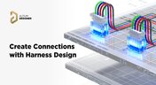
Harness Design
Blog
Create Connections with Harness Design

Many modern electronics have multiple boards, and connecting those different boards and systems together are harnesses. Learn more about how Altium Designer can help you create harnesses for your own multi-board designs here.
Blog
Nucleo Shields Multi-Board Design

Learn how easy it is to create multi-board projects. This practical project article covers the reasons for breaking larger boards into sub-assemblies and explores the various connection options available between sub-assembly boards.
Blog
Analog Solar Tracker Project

In this article you can learn about light sensors while building an analog solar panel tracking system. This open-source project covers multi-channel design, window comparators, driving motors, and photosensors.

Blog
Concept Phase – Initial CAD Design

We are continuing our journey through the open-source laptop project. This article explains an initialization of CAD design process from the early concept and brainstorming phase.
Blog
High-Speed PCB Design Tips

Essential tips for high-speed PCB designs, and when you need to start being concerned about how and where you route your traces.
Introduction to Open Source Laptop Project
Blog
Introduction to Open Source Laptop Project

We have started a very exciting journey into the creation of an open source laptop project. This project will be an ongoing one, with our community able interactively participate. By utilizing Altium 365 users will be able to view, comment on, and download design files. This will be a great learning experience for new and experienced PCB designers.

Blog
Ebook: Routing High-Density Interconnects with Reliable Microvias

HDI PCBs take a particular approach to routing interconnects through multiple layers to ensure reliability during fabrication, assembly, and operation. The critical structure that enables this is microvias, which are prone to failure if not designed properly. In this e-book, readers will receive an initial look at the reasons microvia reliability has come into the spotlight and why HDI PCB designers put reliability first when routing through microvias.

Tag
NEW
Embedded thumbnail for Just Released: Supplier Data Merging
New in Altium's Software
Just Released: Supplier Data Merging

Discover how the Supplier Data Merging feature brings together supplier information from your custom parts database and the Altium Parts Provider into a single, unified view. Access consolidated supplier data wherever supplier part numbers appear, including in ActiveBOM and during component selection.

Embedded thumbnail for How Altium’s Layer Stack Manager Actually Works
How-To's
How Altium’s Layer Stack Manager Actually Works

Take a look inside Altium's Layer Stack Manager and discover how its impedance calculator determines the ideal trace width for your target impedance. In this video, we break down the "black box" behind the calculation and show how the Simbeor-based field solver provides accurate results while eliminating the need for advanced field solver expertise.

Embedded thumbnail for Connect Requirements Directly to Your PCB Design
New in Altium's Software
Connect Requirements Directly to Your PCB Design

See how the Requirements Portal integration in Altium Designer simplifies requirements management by bringing system requirements directly into your PCB design workflow. Connect requirements to design documents, assign tasks, track verification in real time, and keep your entire team aligned with seamless synchronization in Altium 365.

Embedded thumbnail for SFP Connector Routing: High-Speed Differential Pair Design Tips
How-To's
SFP Connector Routing: High-Speed Differential Pair Design Tips

Discover practical SFP and SFP+ routing tips in our latest video, inspired by a real question from the Altium subreddit. We cover how aggressive serpentine length tuning can be, how to reduce impedance discontinuities in tight meanders, and how meandering influences mode conversion at 10G and higher data rates.

Embedded thumbnail for Handle High-Density PCB Layouts with Ease
New in Altium's Software
Handle High-Density PCB Layouts with Ease

Push the limits of PCB design with support for up to 128 signal layers, empowering the development of even the most complex, high-density boards.

Embedded thumbnail for Skip Layer Routing for RF: Control Impedance & Cut Insertion Loss
How-To's
Skip Layer Routing for RF: Control Impedance & Cut Insertion Loss

Discover our latest video and learn how RF designers use a deeper ground plane to minimize skin-effect resistance, improve signal integrity over long high-frequency routes, and optimize impedance matching for oversized SMT pads in antenna launches and coaxial connectors.

Embedded thumbnail for Just Released: ODB++ Intellectual Property Protection
New in Altium's Software
Just Released: ODB++ Intellectual Property Protection

ODB++ Intellectual Property Protection lets you control exactly what design data is included in the ODB++ output, ensuring each manufacturing partner receives only the information needed for their specific fabrication or assembly tasks.

Embedded thumbnail for Future of Electronics Development in Security and Aerospace
How-To's
Future of Electronics Development in Security and Aerospace

See the highlights from Altium's executive event in Hamburg, where Security and Aerospace leaders explored AI-driven development, digital engineering, supply chain resilience, and the future of mission-critical electronics.

Embedded thumbnail for Create Clearance Rules Faster and with Less Effort
New in Altium's Software
Create Clearance Rules Faster and with Less Effort

Setting up clearance rules is now more intuitive in the Constraint Manager. Choose the Simple view for faster configuration with grouped object types, or the Advanced view when you need detailed, matrix-based clearance control.

Embedded thumbnail for Mastering HDI Design Rules in Altium Designer
How-To's
Mastering HDI Design Rules in Altium Designer

In our latest Altium Academy tutorial, we guide you through configuring the essential HDI PCB design rules in Altium's software. You'll learn how to use your manufacturer's fabrication capabilities to create accurate design rules and constraints for your PCB.

Embedded thumbnail for Search, Filter, and Navigate PCB Designs Faster
New in Altium's Software
Search, Filter, and Navigate PCB Designs Faster

The Web Viewer now features a redesigned search experience for faster access to PCB design data across supported CAD formats. A lightweight, intuitive interface lets you begin with simple search terms and progressively refine results using contextual suggestions.

Embedded thumbnail for Gain Better Control Over Wire Bond Visibility
New in Altium's Software
Gain Better Control Over Wire Bond Visibility

New bond wire visibility controls give you greater flexibility when working with wire-bonded boards and footprints, making it easier to focus on the details that matter most.

Embedded thumbnail for Coming Soon: Selectable Harness Source Within Multi-board Design
New in Altium's Software
Coming Soon: Selectable Harness Source Within Multi-board Design

Selectable Harness Source Within Multi-board Design enables harness projects to drive system connectivity while maintaining bidirectional synchronization between multi-board schematics and harness wiring diagrams for improved accuracy and easier design management.

Embedded thumbnail for Choose the Simbeor Version for Your PCB Calculations
New in Altium's Software
Choose the Simbeor Version for Your PCB Calculations

The PCB Editor now lets you choose the Simbeor version used for delay and impedance calculations, giving you more flexibility and consistency across your design workflows.

Embedded thumbnail for Improve PCB Editor Performance with Via Instancing
New in Altium's Software
Improve PCB Editor Performance with Via Instancing

The PCB Editor now uses via instancing to generate geometry for each via individually, providing greater flexibility and a more advanced approach to managing vias in PCB designs.

Embedded thumbnail for GSSG Stackup Deep Dive: Routing, Impedance, and HDI
How-To's
GSSG Stackup Deep Dive: Routing, Impedance, and HDI

A ground-signal-signal-ground (GSSG) stackup rethinks the traditional four-layer PCB structure by moving the ground planes to the outer layers and routing signals on the two inner layers. In this Altium Academy deep dive, we review a real one-minute design review submission and demonstrate how to configure a GSSG stackup properly using the Layer Stack Manager.

Tag
Your search returns no results.