News & Updates

Blog
•
What’s New in Altium 365: Version Control for Hardware, Layer Stackup in Web Viewer, and SOC 2 Type 1 Certification
In February, we hit a new record in the number of users on the platform. The Altium 365 user community is now 20,000 strong! You can now migrate from an external version control system to Altium 365 preserving the history of commits. We also received the SOC 2 Type 1 certification from KPMG, made layer stack available in the web viewer, and added the brand new capability to track tasks in the context of your design project. Keep reading to learn more!


Blog
•
Introducing Spectra's Electronic Design to Delivery Index
Get a cohesive view of supply chain market conditions, stay on top of trends, and avoid disruption with this free, monthly report from Spectra.


Blog
•
Support for Rigid-Flex in Altium Designer
Rigid-flex in Altium Designer starts with designing a manufacturable PCB layer stack complete with via transitions and any calculated impedance requirements. Flex sections also need to be placed in the layer stack before moving into the PCB layout. Once inside the PCB editor, bending lines can be clearly defined in the PCB layout, and these can be visualized in Altium Designer's 3D PCB design tools. Keep reading to see how Altium Designer supports your flex and rigid-flex designs.


Blog
•
Communicating PCB Layer Stackup Needs to Manufacturers
In the business of PCB design, communicating needs to manufacturers and vendors is a top priority. The context of our requests is sometimes lost either by not providing the correct information, not listing enough information, or not giving any information. Although the experienced PCB designer can take steps to specify everything they want to see in their PCB stackup, eventaully the manufacturer will handle that decision in an effort to balance available materials with processing capabilities and yield.

Blog
•
Risk Vs. Reward
During the recent IPC APEX expo, there was a lot of discussion about SAP, or semi-additive PCB processes. As with any new technology adoption there were people that are excited to jump right in and start designing with much finer feature sizes and work through the inevitable changes to the traditional thought process. Others are in a "let’s wait and see" mode and of course there are a few skeptics there as well, so keep reading to learn more.


Blog
•
Parasitic Extraction with an Electromagnetic Solver in PCB Routing
Parasitic extraction: the integrated circuit design community must grapple with this task on a daily basis, especially once gate features are reduced below ~350 nm and chips run at high switching speeds. The PCB community also has to deal with this idea in order to better design power delivery networks, interconnects with precise impedance, and properly quantify crosstalk and coupling mechanisms.


Blog
•
Ebook: PDN Simulation and Analysis Guide
Most designers don’t realize they need to worry about power integrity until they have a power integrity problem. Other designers might build boards that can’t handle the demands of modern digital and high frequency components, and they may not realize the problems that lurk in their power delivery network (PDN). Although the basic concepts involved in designing for power integrity are well-known, myths about power integrity abound, and designers need tools to help them evaluate and qualify power integrity in a PDN.


Blog
•
Ferrite Beads and Transfer Impedance in a PDN Simulation
The use of ferrites in a PDN is one design recommendation that is fraught with unclear guidance and over-generalized recommendations. If you see an application note or a reference design that recommends placing a ferrite in a PDN, should you follow this in your specific design, or should you ignore this and focus on adding capacitance?

Blog
•
Overview of PCB Design Output Files
Before your board can be put into production and prepared for assembly, you have to generate a set of files that assist your manufacturer. These are your PCB design output files, also known as manufacturing files, fabrication data, assembly files, and a host of other names. Before you send your design file off to a manufacturer in an email, make sure to get a list of their required fabrication and assembly files first. If you’re a new designer, take some time to read over the basic PCB manufacturing file extensions below.


Blog
•
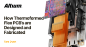
How Thermoformed Flex PCB’s are Designed and Fabricated
Thermoformed flexible PCBs are specially designed and fabricated by heating and molding them into specific shapes, making them suitable for compact and complex applications like automotive dashboards and wearable devices. This process involves precise temperature control and careful handling to ensure durability and quality. Discover more from Tara Dunn's new article.
Blog
•
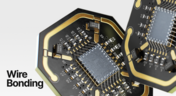
Boost Connection Integrity and Design Efficiency with Wire Bonding
Altium Designer's wire bonding feature enhances PCB design by supporting chip-up configurations for Chip on Board (CoB) designs. It offers easy validation of bond wiring in 3D views, ensuring accurate and efficient design processes. Check more about this feature on Altium's new feature page.
Blog
•
How High Frequency SMD Passives Work in a PCB Layout
High-frequency surface-mount device (SMD) passives like resistors and capacitors play a crucial role in PCB layouts, particularly in circuits operating above 1 GHz. Our article explores how these components function at high frequencies, their operational limits, and the importance of considering parasitic elements in design.

Blog
•
Essential DFM Tips for Aerospace Projects
Design for Manufacturing (DFM) is a crucial aspect of aerospace projects. This process ensures high-quality designs that meet the unique challenges of the aerospace industry, such as extreme conditions and stringent reliability standards. Learn more about essential DFM tips in our brand-new article.
Blog
•
Mechanics Meet Electronics Seamlessly in Multi-Board PCB Design
Curious about the intersection of mechanical and electrical design? Both are crucial in the PCB design process, especially for multi-board systems. Read our latest article to learn how ECAD and MCAD can address significant challenges during PCB preparation.

Blog
•
Altium 365 now has its own website!
Discover everything you need to know about Altium 365 and experience our suite of applications for secure, seamless, and streamlined collaboration. Visit now to explore how to streamline your electronic product development.
Blog
•
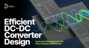
Efficient DC-DC Converter Design: Automated Measurements with Altium Designer 24 MixedSim
Automated measurements are no longer tough. With our Mixed Simulation mode, everything is easier. Learn more about this feature based on DC-DC buck converter design in this brand new article.
Blog
•
Altium Designer: Leading the Charge in PCB Design Innovation
In the dynamic field of electronics design, Altium Designer stands out as a pioneer, continuously advancing the boundaries of PCB (Printed Circuit Board) design. Discover the latest innovations in 3D-MID design, high-speed design, and interactive routing in this new article by David Marrakchi.
Blog
•
What Is Solder Mask Expansion and Which Value Should You Use?
Check out our new article explaining how to ensure sufficient pad area for soldering, manage misregistration tolerance, and maintain proper solder dams between components. It also highlights the role of collaboration with fabrication houses and the use of CAD tools in defining land patterns for advanced electronics designs.
Blog
•
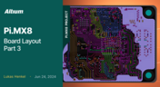
Pi.MX8 Project - Board Layout Part 3
We continue our exploration of the Pi.MX8 open-source computer module project. In this new installment, we focus on routing planning and then cover all the layers' routing with all the details you need to know if you want to prepare a similar project.

Blog
•
Mastering Blind and Buried Vias
Check our compilation of essential resources you'll need to use blind and buried vias successfully in an HDI PCB. In our brand new article, we present the main and most valuable information about this technology, which may not be new but is still highly useful in High-Density Interconnect projects.

Blog
•
Penn Electric Racing Pushes the Envelope with Altium 365
Discover how Penn Electric Racing builds award-winning, fully electric racecars with Altium 365, pushing the boundaries of technology and design.
Blog
•
Make Sure to Clean Your No-Clean Flux
No-clean flux has become popular due to its convenience. Learn more about why this solution is used, why cleaning might still be necessary, and how to remove no-clean flux residues. We will try to dispel all these doubts in this brand new article.

Blog
•
SPICE Simulation Module: How To Use Automated Measurements in Simulations To Save Time and Money in Design Challenges
Simulation of electronic circuits is a key factor in the success of your design. A SPICE circuit simulator may be used to speed up the design analysis. Learn more about how Altium Designer can help you with automated measurements, saving you time and money during the design process.
Blog
•
Achieve Seamless Rigid-Flex Design with Altium Designer's Unified Solution
Check out our refreshed feature page about Rigid-Flex PCB Design and see how Altium Designer’s unified environment can help you manage this kind of project with no limitations or additional licensing required.

Blog
•
How to Design a Thermal Prototype PCB
Thermal problems in PCBs often go unnoticed until prototyping, which can be costly. Design teams can't afford endless iterations, but they can conduct lower-cost thermal prototypes. Learn more about this approach in our new article.
















Your search returns no results.


