News & Updates

Blog
•
A-SAP™ – What do you need to know?
The continued miniaturization of both packaging and component size in next-generation electronics is becoming harder and harder to work around and presents a significant challenge for both PCB designers and PCB fabricators. To effectively navigate the constraints of the traditional subtractive-etch PCB fabrication processes, PCB designs require advanced PCB fabrication capabilities while pushing the limits of finer feature size, higher layer counts, multiple levels of stacked micro vias and increased lamination cycles.


Blog
•
Pin-Package Delay and Via Delay in High Speed Length Tuning
Take a look at the inside of some integrated circuit packages, and you’ll find a number of wires bonded to the semiconductor die and the pads at the edge of the component's package. As a signal traverses makes its way along an interconnect and into a destination circuit, signals need to travel across these bond wires and pads before they are interpreted as a logic state. As you look around the edge of an IC, these bond wires can have different lengths, and they incur different levels of delay and contribute to total jitter.


Blog
•
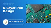
6-Layer PCB Design Guidelines
Once you’ve run out of room on your 4-layer PCB, it’s time to graduate to a 6-layer board. The additional layer can give you room for more signals, an additional plane pair, or a mix of conductors. How you use these extra layers is less important than how you arrange them in the PCB stackup, as well as how you route on a 6-layer PCB. If you’ve never used a 6-layer board before, or you’ve had EMI troubles with this stackup that are difficult to solve, keep reading to see some 6-layer PCB design guidelines and best practices.
Blog
•
Altium Designer 22.5 Update
We are happy to announce that the Altium Designer 22.5 update is now available. Altium Designer 22.5 continues to focus on improving the user experience, as well as performance and stability of the software, based on feedback from our users. Check out the key new features in the What's New section on the left side of this window!

Blog
•
How Reliable is Your Hybrid PCB Stackup?
PCB stackups often incorporate slightly dissimilar materials that could pose a reliability problem. Hybrid PCBs are one case where the PCB stackup will include different materials, typically a standard FR4 laminate and a PTFE laminate for RF PCBs. Designers who want to take the lead on material selection when designing their hybrid stackups should consider these factors that affect reliability. As with any PCB stackup, make sure you get your fabricator involved in the manufacturing process early to ensure reliability problems do not arise during production.


Blog
•
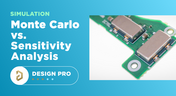
Monte Carlo Simulation vs. Sensitivity Analysis: What’s the Difference?
In a previous article about circuit simulation and reliability, I looked at how Monte Carlo analysis is commonly used to evaluate circuits that are subject to random variations in component values. Sensitivity analysis is a bit different and it tells you how the operating characteristics of your circuit change in a specific direction. Compared to a Monte Carlo simulation, sensitivity analysis gives you a convenient way to predict exactly how the operating characteristics will change if you were to deliberately increase or decrease the value of a component.

Blog
•
Creating Continuous Integration Pipelines for FPGAs
Field Programmable Gate Arrays, or FPGAs, have become ubiquitous amongst high-speed, real-time digital systems. The speed at which FPGAs operate continues to increase at a dizzying pace but their adoption into Continuous Integration pipelines seems not to trail as closely. In this article we will review the concept of CI pipelines, their application to FPGAs, and look at examples on how to set this up.


Blog
•
Soft Locks [Conflict Prevention] in Altium 365
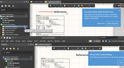
Conflicts can occur when multiple people work on the same project simultaneously. The user might not realize that they are not looking at the latest version of the documentation, leading to problems later. To address this issue, Altium features an intuitive graphical user interface that allows you to examine conflicts quickly and carefully

Blog
•
The Basics of Monte Carlo in SPICE: Theory and Demo
Anytime you place a component in your PCB, it’s almost like you’re gambling. All components have tolerances, and some of these are very precise, but others components can have very wide tolerances on their nominal values. In the event the tolerances on these components become too large, how can you predict how these tolerances will affect your circuits?



Blog
•
What's In Your BGA Land Pattern and Footprint
If you look in datasheets for most components, you’ll often find a recommended land pattern, usually alongside some mechanical package information and assembly information. This is not always the case with BGA components, especially components with high ball count. There are a few reasons for this that we can speculate: those ball counts might just be too big to put into a single page, or the manufacturer just expects you to know how to create that land pattern.

Blog
•
PCB Via Current-Carrying Capacity: How Hot is Too Hot?
One common question from designers is current-carrying capacity of conductors in a PCB. Trace and via current-carrying capacity are legitimate design points to focus on when designing a new board that will carry high current. The goal is to keep conductor temperatures below some appropriate limit, which then helps keep components on the board cool. Let’s dig into the current state of thermal demands on vias in PCBs and how they compare to internal and external PCB traces.

Blog
•
Phalanx, not Failure: PCB Shielding to Protect Your Design
A combination of good printed circuit board design and good shielding mitigates EMI. Good PCB design for EMI shielding revolves around the layout, the placement of filters, and ground planes. A well-designed PCB minimizes parasitic capacitance and ground loops. Keep reading to learn more about PCB shielding.
Blog
•
Best Practices in Hardware Version Control Systems
Any project can get very complex, and the PCB design team needs to track revisions throughout a project. Why worry about tracking revisions? In the event you ever receive changes to product functional requirements, major changes are made to your product’s architecture, or you’re ready to finalize the design and prepare for fabrication, it’s best to clone a project at its current state and begin working on a new version. Keeping track of all these design changes in a PCB design project takes the type of hardware version control tools you’ll find in Altium 365™.

Blog
•
Copper Pour and Via Stitching: Do You Need Them in a PCB Layout?
To pour or not to pour, to stitch or not to stitch… Over many years, some common “rules of thumb” have become very popular and, ultimately, taken a bit out of context. Rules of thumb are not always wrong, but taking PCB design recommendations out of context helps justify bad design practices, and it can even affect the producibility of your board. Like many aspects of a physical PCB layout, via stitching and copper pour can be like acid: quite useful if implemented properly, but also dangerous if used indiscriminately.
Blog
•
Should You Use Power MOSFETs in Series?
Power MOSFETs enable a huge range of electronic systems, specifically in situations where BJTs are not useful or efficient. MOSFETs can be used in high current systems in parallel arrangements, but what about their use in series? Both arrangements of MOSFETs have their pitfalls that designers should consider. Let’s look at MOSFETs in series as they are quite useful in certain systems, but be careful to design your circuits and your PCB for reliability.

Blog
•
Controlled ESR Capacitors: Should You Use Them for Power Integrity?
I can’t think of a single product I’ve built that doesn’t require capacitors. We often talk a lot about effective series inductance (ESL) in capacitors and its effects on power integrity. What about effective series resistance (ESR)? Is there a technique you can use to determine the appropriate level of resistance, and can you use ESR to your advantage?
Blog
•
Microstrip Ground Clearance Part 2: How Clearance Affects Losses
If your goal is to hit a target impedance, and you’re worried about how nearby pour might affect impedance, you can get closer than the limits set by the 3W rule. But what are the effects on losses? If the reason for this question isn’t obvious, or if you’re not up-to-date on the finer points of transmission line design, then keep reading to see how nearby ground pour can affect losses in impedance-controlled interconnects.
Blog
•
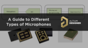
Choosing the Right Microphone for Embedded Applications
If you need to capture sound waves for your electrical device to process, you'll need a microphone. However, microphones these days have become very advanced, and there are so many options to choose from. They range from the relatively simple and popular condenser type microphones to state-of-the-art sound conversion solutions incorporating internal amplifiers and other electronic processing functionality. In this article, we'll take a look at some of the options available.

Blog
•
Composite Amplifiers and How They Give the Best of Both Worlds
There are many times where you need an amplifier with high gain, low noise, high slew rate, and broad bandwidth simultaneously. However, not all of these design goals are possible with all off-the-shelf components. Here are some points to consider when working with a composite amplifier design and how to evaluate your design with the right set of circuit simulation tools.
Blog
•
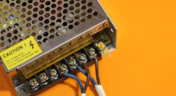
Reduce Common-Mode Noise in Your Power Supply with Impedance Balancing
Simple switching regulator circuits that operate in compact spaces, like on a small PCB, can usually be deployed in noisy environments without superimposing significant noise on the output power level. As long as you lay out the board properly, you’ll probably only need a simple filter circuit to remove EMI on the inputs and outputs. As the regulator becomes larger, both physically and electrically, noise problems can become much more apparent, namely radiated EMI and conducted EMI in the PCB layout.

Blog
•
Part 1: Why Your PCB Design Review Process Is Obsolete and What You Can Do About It
A PCB design review is a practice to review the design of a board for possible errors and issues at various stages of product development. It can range from a formal checklist with official sign-offs to a more free-form inspection of schematic drawings and PCB layouts. For this article, we will not delve into what to check during a design review process but rather look at how a review process itself usually unfolds and how to optimize it to get the most out of your time.
Blog
•
Part 2: Why Your PCB Design Review Process Is Obsolete and What You Can Do About It
As we established in Part 1, the PCB design review and collaboration practices have room for improvement in many organizations. To address this, we developed Altium 365. Let's examine how running a PCB project through Altium 365 compares to other methods.

Blog
•
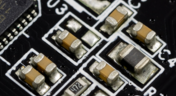
What is PCB Star Grounding and Why Would Anyone Use It?
If you look on the internet, you'll find some interesting grounding recommendations, and sometimes terminology gets thrown around and applied to a PCB without the proper context or understanding of real electrical behavior. DC recommendations get applied to AC, low current gets applied to high current, and vice versa... the list goes on. One of the more interesting grounding techniques you'll see as a recommendation, including on some popular engineering blogs within the industry, is the use of PCB star grounding.
Blog
•
Your Guide to PCB Silkscreen
Every PCB has silkscreen on the surface layer, and you’ll see a range of alphanumeric codes, numbers, markings, and logos on PCB silkscreen. What exactly does it all mean, and what specifically should you include in your silkscreen layer? All designs are different, but there are some common pieces of information that will appear in any silkscreen in order to aid assembly, testing, debug, and traceability
Blog
•
What Causes Gibbs Ringing in High-speed Channel Simulations?
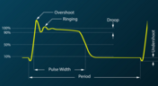
Designing high-speed channels on complex boards requires simulations, measurements on test boards, or both to ensure the design operates as you intend. Gibbs ringing is one of these effects that can occur when calculating a channel’s response using band-limited network parameters. Just as is the case in measurements, Gibbs ringing can occur in channel simulations due to the fact that network parameters are typically band-limited.
Blog
•
Efficient Heat Dissipation with SMD Heat Sinks Keeps You From Dropping PCBs
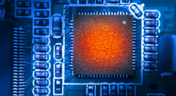
In electronics, there is the possibility that your PCB can get pretty hot due to power dissipation in certain components. There are many things to consider when dealing with heat in your board, and it starts with determining power dissipation in your design during schematic capture. If you happen to be operating within safe limits in a high power device, you might need an SMD heat sink on certain components. Ultimately, this could save your components, your product, and even the operator.







Your search returns no results.


