News & Updates

Blog
•
The Positive Impact of Supply Chain Visibility on Design to Cost
Design to cost is a lofty idea that is only perfectly executed when supply and demand for components are in perfect harmony. Unfortunately, the current landscape for component sourcing makes design to cost more of a balancing act rather than an exercise in price reduction. To help designers in their efforts to balance cost, capabilities, and procurement, we created this ebook to help users understand how modern supply chain tools can help in these complex design problems.

Blog
•
A Brief Study of Stubs on a PCIe Connector
Stubs are an important topic in high-speed PCB design, and there is a longstanding guideline that stubs should always be removed from all vias on high-speed digital interconnects. While stubs are bad for high-speed lines, they do not always need to be removed. What is more important is to predict the loss profile and frequencies, and to floorplan appropriately to try and prevent such losses.



Blog
•
PCB Layout Cleanup Before Manufacturing
Once you finish your placement and routing in your PCB layout, it can be tempting to wrap up the layout and send everything in directly to manufacturing. The reality is that the board may still need some work before it is considered finished. The cleanup you perform at the final stage of PCB layout will help you catch any outstanding errors that can't be programmed into your DRC engine, and it gives you a chance to add any outstanding details to the surface layers.


Blog
•
Insulated Metal Substrates: Building an LED Panel
In this project we’ll be building a moderate sized LED panel on insulated metal substrate (IMS). This light panel has three different white balance High CRI LED types on it, warm, neutral and cool. By changing the brightness of the different white balances, the light from the panel can be adjusted to match other lighting, making it perfect for film use - but also creating perfect lighting for electronics work. As with all my projects, this LED panel is open source, you can find the Altium project files over on my GitHub released under the permissive MIT License.


Blog
•
DFM in PCB Material Selection
Every design should begin with selecting the materials that will appear in the PCB stackup, as well as arranging layers in the stackup to support layout and routing. This section of our PCB manufacturing andc DFM crash course focuses on selecting the right materials for your PCB design. Materials should be selected given the particular design requirements outlined in your specifications.

Blog
•
How to Start an FPGA PCB Layout For Your Embedded System
FPGAs come in quad or BGA packages that can be difficult to floorplan, especially with the high number of I/Os often implemented in these components. FPGAs offer a lot of advantages in terms of their reconfigurability, but they can require a lot of effort to layout and route without headaches. If you’ve never worked with an FPGA in your PCB layout, we have some guidelines that can help you get started.



Blog
•
How to Get 3-port S-parameters From a 2-port VNA Measurement
S-parameters are fundamental quantities in signal integrity, and an ability to understand them from measurement or analysis is very important. If you have a 3-port network, like a power divider or circulator, it may appear that you must use a 3-port VNA to measure these S-parameters. It is always acceptable to measure between two ports, but you need to know what exactly it is you are measuring. In this article, we’ll look at the relationship between the true 3-port S-parameters with a 2-port measurement.


Blog
•
A Day in the Life of the PCB Manufacturing Process
Before implementing design for manufacturing, it is important to understand the underlying process behind producing a physical PCB. Regardless of the various technologies present in each facility, a large majority of industry-leading manufacturers follow a specific set of steps to turn your design from a drawing in a CAD application into a physical board. In this article, we'll cover the basics that designers need to know as part of our crash course series on PCB manufacturing.



Blog
•
Addressing Skew Sources in High Speed PCBs
If you compile a list of skew sources, you'll see that fiber weave-induced skew is only one entry on a long list of skew sources. We'll look at this list of possible skew sources below, and we'll see how they affect the operation of your PCB. From the list below, we'll see that some of these issues with skew are not simply solved by paying attention to the fiber weave construction in a PCB substrate.
Blog
•
Should Ground Be Placed Below Inductors in Switching Regulators?
We love answering questions from our readers and YouTube viewers, and one of the recent questions we received relates to EMI from switching elements in a switching regulator is "Should a cutout be placed below the inductor in a switching regulator circuit?". Despite the variations in inductors and their magnetic behavior, there are some general principles that can be used to judge the effects of placing ground near inductors in switching regulator circuits. We’ll look at some of these principles in this article
Blog
•
Using Altium 365 Over Your Vanilla Version Control System
There are all sorts of version control systems (VCS) out there that people have been using with their PCB design software. As discussed in Why Use a Version Control System, we looked at different options ranging for local hard drive storage to sophisticated online revisioning systems. In this article we will be reviewing the differences between a standard VCS and Altium 365.

Blog
•
Recover Conductor Losses By Clearing Your PCB Ground Layer
Controlled impedance routing at high frequencies is difficult enough, and it's important to make sure that you stay within your loss budget on long routes or in lossy media. When you have to route a long trace or a long differential pair to a connector or another component, what can you do if you're reaching the end of your loss budget? In this article, we’ll take a look at the skip reference routing method and explain how it can help recover some loss budget in a lossy interconnect.
Blog
•
Announcing SOC 2 Type 1 Certification for Altium 365
We are pleased to announce that Altium 365 is officially SOC 2 Type 1 certified. System and Organization Controls (SOC) 2 is a widely recognized attestation of security compliance defined by the AICPA and is considered the standard for ensuring data security and operational maturity. A SOC 2 certification provides valuable information for companies to assess the quality of the security provided by a service such as Altium 365.

Blog
•
Improving Supply Chain Success with BOM Management
It’s no secret that component shortages have become more frequent this year. Companies will continue to grapple with supply chain challenges into 2022 and beyond. The impact of manufacturing delays can be substantial if a part is not available. Delays occur and sales plans get put on hold. It can also be very expensive and risky to replace parts from multiple sources. Fortunately, many shortages can be avoided by introducing proactive supply chain practices.

Blog
•
Overview of PCB/PCBA Reliability and Failure Analysis
Reliability testing and failure analysis of a PCB/PCBA go hand-in-hand; when designs are stressed to the limit, their failure modes need to be determined through thorough inspection and analysis. To get started on this topic, it’s important to understand the qualification aspects that will govern your bare board design and the PCBA. We’ll look at the various dimensions of PCB/PCBA reliability, as well as some of the standard failure analysis techniques used to identify potential design change requirements.

Blog
•
When Do PCB Power Plane Resonances Occur?
By now, designers should be aware of some important behavior involved in power delivery to components in a PCB, particularly for digital components. All digital components produce and manipulate wideband signals, where the frequency content theoretically extends up to infinite frequency. As such, some radiation may propagate through your PCB, leading to resonant behavior that is not observed on the power rail.

Blog
•
How to Choose PCB Plating for Your Finished Board
Once your board passes through the standard PCB fabrication process, the bare copper in your PCB will be ready for the application of a surface finish. PCB plating is applied to protect any copper in your PCB that would be exposed through the solder mask, whether it’s a pad, via, or other conductive element. In this article, I’ll run over the different PCB plating material options and their advantages in your PCB.

Blog
•
What is the PCB Supply Chain?
The PCB supply chain encompasses multiple components, raw materials, and the PCB itself. PCBs and PCB assemblies are often the most technically complex components that are purchased for electronic assemblies and products. The complexity of modern PCBs leads to several challenges for a supply chain management team that may be significantly different when compared with other commodities the team manages. In this brief guide, we'll look in-depth at the PCB supply chain, and specifically what falls within the purview of a procurement and supply chain management team.

Blog
•
A Guide to Mode Conversion, Its Causes, and Solutions
On interconnects, such as board-to-board connections or cascaded transmission line arrangements, you have an important EMC compliance metric that is sometimes overlooked. This is mode conversion, which can be visualized in an S-parameter measurement for differential and common-mode signal transmission. In this article, we’ll look at a short overview of mode conversion in high-speed design with some examples from common differential standards.

Blog
•
PCB Via Size and Pad Size Guidelines
There are some aspects of PCB design and layout that seem deceptively simple, and yet they have a complex answer that is related to many important aspects of manufacturing. One of these design aspects is the match between PCB via size and pad size. Obviously, these two points are related; all vias have a landing pad that supports the via and provides a place to route traces into a via pad. However, there are some important sizing guidelines to follow when the matching pad and via sizes, and this match is an important element of DFM and reliability.
Blog
•
Differential Microstrip Impedance Calculator
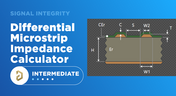
Are you looking for a free tool that you can use to calculate the impedance of differential microstrips? We created a simple tool you can use to calculate differential microstrip impedance for a given geometry and dielectric constant. If you’ve been looking for an accurate differential microstrip impedance calculator, then the calculator below is certainly one of the best free tools you’ll find on the internet before you start using field solvers to determine differential pair impedance.

Blog
•
Getting Through a PCB DFM Check
In this article, we’ll discuss the key design features to implement, and steps to take prior to fabrication that will help prevent some common DFM problems. I’ll also provide examples of where I commonly see these PCB DFM problems in signal integrity circuits.

Blog
•
What is Spreading Inductance?
If you’re working with a high-speed digital component, there are some simple power integrity rules that should be followed. However, there is one quantity that is sometimes ignored when building a PDN impedance simulation: the spreading inductance of your plane pair. Here are some points designers should know about the spreading inductance of a plane pair.

Blog
•
PCB Design Basics for New Designers
In this article, I’ll present some design basics that every new designer should follow to help ensure their design process is successful. Some of these points may challenge the conventional view of how circuit boards are constructed, but they are intended to help balance low noise signaling, manufacturability, and ease of solving a layout.

Blog
•
Selecting Materials for High Voltage PCB Design and Layout
High voltage PCBs are subject to certain safety and reliability concerns that you won’t find in most other boards. If your fabrication house specializes in high voltage PCBs and keeps materials in stock, they can likely recommend a material set, as well as a standard stackup you might use for certain voltage ranges and frequencies. If you need to choose your own materials, follow the tips below to help you narrow down to the right material set.

Blog
•
When to Use Tented Vias in Your PCB Layout
There are some guidelines I see many designers implement as a standard practice, often without thinking about it. Some of these practices are misunderstood or implemented without best practices. Others are implemented without thinking about the potential problems. One of these is the use of tented vias, which is sometimes implemented in a PCB layout by default. Is this always the right practice?


Your search returns no results.


