News & Updates

Blog
•
Can You Fix a Warped PCB?
Before we get too deep into this article, I’ll give you the simple answer. You probably can’t fix warping in your PCB after it’s already been fabricated. You can prevent an unwarped board from becoming warped during assembly, but only as long as materials were selected properly and the board is put into reflow correctly. We’ll run over some of these points in this article, and I’ll examine some points that might help you recover a warped board.

Blog
•
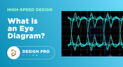
What is an Eye Diagram?
The eye diagram is a useful measurement or simulation as part of channel compliance. The measurement shows many different factors that can affect signal behavior simultaneously, ultimately allowing for qualification of errors and losses in a channel. In this article, I’ll run over some of the fundamental measurements that you could manually extract from an eye diagram and how they reveal some strategies for improving channel designs.

Blog
•
What Skills Are Needed to be a PCB Layout Designer?
To readers who have been working in the PCB industry for most of your career, you have probably seen a very diverse group of professionals with varied skill sets and backgrounds. Designers might get started as engineers or as technicians, and some designers learn how to create beautiful PCB layouts in university. No matter how you got into PCB design, there are some important skills to know that will take you a long way towards advancing your career.

Blog
•
Beginner PCB Design Mistakes and How To Avoid Them
When starting out with PCB design, it’s common to treat the process as simply ‘connecting the dots’: as long as connections are made, it’s not particularly important how these connections are made. Having reviewed quite a number of PCBs of other PCB design engineers over the last few years, there are common, unfortunately erroneous, occurrences between a lot of them. This article aims to illustrate the top five beginner PCB design mistakes and what we can do to avoid making them. Let’s get started!
Blog
•
SAP (Semi-Additive PCB Process) – Top 5 Questions Regarding Stack Up
As the PCB design community embraces the benefits of this new printed circuit board fabrication technique, there are of course many questions to be answered. Today’s blog will address some of the most commonly asked questions related to circuit layer stack up as people are introduced to this new technology.

Blog
•
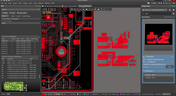
Altium Designer 22.9 Update
We are happy to announce that the Altium Designer 22.9 update is now available. Altium Designer 22.9 continues to focus on improving the user experience, as well as performance and stability of the software, based on feedback from our users. Check out the key new features in the What's New section on the left side of this window!
Blog
•
Dual Rail Voltage Supply
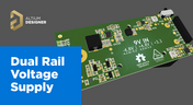
The highest performing operational amplifiers often need a split supply with positive and negative voltages connected to the op amps supply rails. In this project, we’re going to be building a positive/negative dual rail power supply for a differential oscilloscope probe I’m designing. I’m making the power supply a separate project, as a dual rail supply is quite useful to have, and I’m sure I’ll find multiple uses for it in the future.


Blog
•
Library Importer Improvements (former Library Migrator)
Importing file-based libraries from your local computer or network drive to your Altium 365 workspace can be done using the Library Importer. Altium’s Library Migrator was renamed Library Importer—the feature’s name was changed to conform more closely to the tool’s purpose. Not only is its name new, but our team has also made several user experience improvements. We have updated the documentation to reflect this change.
Blog
•
How to Select Copper Foil for High-Frequency PCB Design
The PCB materials industry has spent significant amounts of time developing materials that provide lowest possible signal loss for products with RF applications. For high speed and high frequency designs, losses will limit signal propagation distance and distort signals, and it will create an impedance deviation that can be seen in TDR measurements. In this article, we'll look at the balance between copper foil losses and other types of losses in a PCB, as well as some strategies that are commonly used to overcome roughness.

Blog
•
Altium Designer 22.8 Update
We are happy to announce that the Altium Designer 22.8 update is now available. Altium Designer 22.8 continues to focus on improving the user experience, as well as performance and stability of the software, based on feedback from our users. Check out the key new features in the What's New section on the left side of this window!
Blog
•
What is Hybrid Beamforming?
In this article, we’ll look at beamforming implementation in an advanced method combining analog and digital techniques, known as hybrid beamforming. This method blends both digital and analog techniques to create multiple beams and thus reach multiple users with varying intensities. In the case of an RF imaging system or a radar system, hybrid beamforming in a MIMO technique also allows tracking of multiple targets with adjustable resolution.
Blog
•
Why Most Via Impedance Calculators Are Inaccurate
The problem with every via impedance calculator that I have seen is simple: they are incomplete or totally wrong. The “incomplete” part refers to a lack of context; these calculators can roughly reproduce a well-known estimate from a legend like Howard Johnson in his Digital Design textbooks. However, these calculators never provide insight into what they are actually calculating, or where the calculated via impedance is accurate. Keep reading to see why these calculators get it so wrong, as well as the context surrounding via impedance.


Blog
•
Mastering EMI Control in PCB Design: How to Choose the Stackup for EMC Design
This article by Dario Fresu, part of the Mastering EMI Control in PCB Design series, explores strategies for selecting PCB stackups to optimize EMC performance. It offers actionable tips for balancing cost, manufacturability, and signal integrity in your designs.

Blog
•
AI Vision with the Kria KV260 Vision AI Starter Kit
Discover AI-driven vision capabilities with the Kria KV260 Vision AI Starter Kit, presented by Ari Mahpour. Ideal for prototyping vision solutions, this kit offers an accessible entry point into advanced AI applications.

Blog
•
Model-Based Systems Engineering in the Era of Digital Twins: A Paradigm Shift in PCB and Electronics Design
Explore how Model-Based Systems Engineering (MBSE) integrates with digital twins to enhance design accuracy, collaboration, and lifecycle management in modern engineering projects. This approach bridges the gap between physical systems and digital models, enabling real-time simulation and optimization.
Blog
•
Wire Bonding in Altium Designer
The Wire Bonding in Altium Designer article highlights how Altium Designer 25’s wire bonding feature streamlines complex designs for advanced assemblies like 3D stacked dies and RF modules. This tool enhances efficiency and precision, catering to modern electronic design needs.
Blog
•
Altium Designer 25: Pioneering Collaboration, Product Development, and Advanced Simulation
Altium Designer 25 introduces groundbreaking features for seamless collaboration and precision in PCB design, from PCB CoDesign to advanced simulation and MCAD tools. Discover how AD25 is transforming electronic product development.
Blog
•
Wire Bonding: Modern Applications, Technology Trends and Cost Considerations
Explore the future of wire bonding, from new applications to cost-saving trends, in this article by Samer Aldhaher. Stay updated on key innovations in this essential connection technology.
Blog
•
Maximizing Efficiency: A Deep Dive into Altium 365 Jira Integration Features
Discover how Altium 365’s Jira integration can streamline collaboration and keep projects running smoothly with real-time design updates and task tracking. Perfect for teams seeking efficiency!
Blog
•
Optimize PCB Design with Integrated BOM and CAD Systems
Discover how integrating BOM management and CAD systems can streamline your PCB design process in this insightful article. Learn how combining these tools enables smoother collaboration, reduces errors, and improves design efficiency, helping you optimize your workflows from concept to manufacturing.
Blog
•
The Essential Guide to Through-Hole Resistors
Resistors are fundamental components in electronic circuits, essential for controlling current and voltage. This article explores their basic principles, types, and key applications, helping you understand their crucial role in electronics.
Blog
•
Avoiding Costly Delays: Essential Tips for PCB Designers
Efficient PCB design is crucial for avoiding costly delays in product development. This article offers practical tips and best practices for PCB designers to streamline their workflows, minimize errors, and ensure timely project completion.
Blog
•
Understanding Signal Reflections for High-Speed Design
Signal integrity is the backbone of high-speed digital systems. In this new article by Rafał Stępień, we break down signal reflections and how to optimize your designs with effective impedance matching techniques.
Blog
•
Mastering EMI Control in PCB Design: Component Placement for EMC
In the second article of the "Mastering EMI Control in PCB Design" series Dario Fresu explores how effective component placement can reduce electromagnetic interference (EMI) in printed circuit boards. He highlights strategies such as board segregation and careful management of high-speed signals and their harmonics to ensure signal integrity and minimize emissions.
Blog
•
Signal Integrity Principles based on Altium Designer 24
Check out this article where Rafał Stępień dives into the essentials of maintaining signal integrity in high-speed digital systems. Discover key techniques like controlling signal reflections, reducing crosstalk, and designing differential pairs in Altium Designer 24 to ensure reliable and efficient PCB performance.

Blog
•
Launch of Requirements & Systems Portal in Altium 365
The Requirements & Systems Portal is now live in Altium 365! Engineers can write, manage, and verify requirements within the Altium 365 workspace. You can link your requirements directly to schematics and PCB designs to ensure all engineers are working with the latest data. Request access today!
Blog
•
Enhancing Signal Integrity in PCB Design: Key Considerations and Strategies
Looking to enhance signal integrity in your PCB designs? Check out our latest article by David Marrakchi, where he shares key strategies and best practices for achieving reliable high-speed designs.
Blog
•
Favorite Tools for BOM Review
Check out our article, where Lawrence Romine shares his top tools for conducting efficient Bill of Materials (BOM) reviews in PCB design. It highlights key features in Altium 365, Octopart, and ActiveBOM that help engineers avoid unsourceable components and streamline procurement.
















Your search returns no results.


