News & Updates
Blog
•
Fragmented Feedback Loops: The Hidden Cost in PCB Design and Testing
Explore the hidden impact of fragmented feedback loops in PCB design and testing. Check how minor communication gaps lead to significant financial burdens and learn how to address them.


Blog
•
Altium 365 GovCloud 101: Everything You Need to Know
Would you like to improve the protection of your data? Altium 365 GovCloud can help you achieve these goals. It’s a version of Altium 365, engineered to meet the stringent demands of US government regulations.


Blog
•
Design Phase – Lid Assembly Mechanics Part 3
We are heightening the anticipation for our Open Source Laptop project. In this chapter, we delve into the ambient light sensor module. Learn more about how to implement it into this project.
Blog
•
PCB CoDesign: Design Faster Together
Experience accelerated design collaboration with PCB CoDesign, exclusively available on Altium Designer starting from December 13th. This innovative feature adopts a collaborative approach by seamlessly integrating schematic and PCB design, enabling multiple engineers to work on the same project. Explore this cutting-edge feature on our newly launched page dedicated to its functionalities.

Blog
•
6 Steps to Accelerate the Development of Complex Products
Learn the key lessons from the presentation at Iteration22; “Joe Justice, Wikispeed - Everyone Must Be a Chief Engineer at SpaceX.” Read on and discover how to speed up the development of complex products.
Blog
•
Design Phase – Lid Assembly Mechanics Part 2
We are continuing our journey into lid assembly mechanics inside the Open Source Laptop Project. In this chapter, we are focusing on the sensor PCB above the display panel.


Blog
•
How to Speed Up Your Manual Assembly Process with Assembly Assistant? The Story of XVP Photonics
Are you struggling with your manual assembly process? Would you like to speed it up and improve component placement accuracy? Read the story of XVP Photonics; with Assembly Assistant, they improved the component placement time by 25%. Discover how!
Blog
•
45V-5A Adjustable Half-Bridge DC to DC Converter
DC-to-DC buck converters are extensively employed in electronic devices. In this article, we will introduce you to one of our new projects—a DC-to-DC converter designed to serve as a power supply as well.

Blog
•
The Challenges of Modern Design: Why Requirements Management Is Essential
You need a robust requirements management process to ensure your design intent communication stays clear and organized. Read on to explore the crucial connection between well-managed requirements and today’s design.

Blog
•
Efficiency And Noise Top 10 Switching Regulator Modules
Switching regulator modules have become indispensable in a wide array of electronic devices, providing a more efficient means of voltage conversion between different levels by storing and releasing energy. Explore further insights into these devices in today's dynamic world of electronics.

Blog
•
Add USB Type-C Power Delivery to Your Designs!
We want to invite you to explore the fundamentals of USB Type-C Power Delivery which is now the most popular energy transmission in current times. We will show you how to easily incorporate a dedicated PD IC into your own designs.

Blog
•
Design Phase – Lid Assembly Mechanics Part 1
It is time to delve deep into the mechanical design of our Open Source Laptop project. In this article we give you an update about the first part of fitting elements into the system. You will learn more about laptop lid, webcam integration, light sensor and microphones which will be used in this project.


Blog
•
PCB Via Current-Carrying Capacity: How Hot is Too Hot?
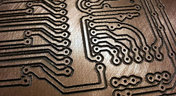
Trace and via current-carrying capacity are legitimate design points to focus on when designing a new board that will carry high current. The goal is to keep conductor temperatures below some appropriate limit, which then helps keep components on the board cool.
Blog
•
How to Maximize Copper in Your PCB Design: The Pros and Cons of Copper Pouring Versus Placing
There is a saying in copper pour PCB design, “Copper is free.” It means a PCB editor designer must think in reverse. A board starts off as solid copper, and the copper you don’t want is removed. It is faster to build, less consumptive, and less expensive to make a board that is mostly copper as compared to the same size board that is mostly bare. Picking the correct technique will make the difference between an effortless or frustrating experience.

Blog
•
Top 5 PCB Design Guidelines Every PCB Designer Needs to Know
What’s the key to designing a board that’s realistic on paper and in physical form? Let’s explore the top 5 design guidelines that you need to know to design your next manufacturable, functional and reliable PCB.
Blog
•
5月 14, 2020
How to Highlight Nets in Altium Designer to Simplify Schematic and PCB Designs
Highlighting nets will help you simplify your schematic and PCB design. In Altium , there are multiple options that enable you to leverage this capability to simplify the verification of connections and circuit paths and make sure that the design you send to your manufacturer accurately reflects the printed circuit board you need built.

Blog
•
5月 12, 2020
Keep Your Altium Designer PCB Layout in Line with Grids and Grid-Selection Shortcuts
The grid system in a printed circuit board design CAD system really is your friend, and if you haven’t taken the time to get properly introduced yet let me help you with that.

Blog
•
5月 7, 2020
How to Panelize Your PCBs Before Lunch with Altium Designer
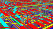
Whether you have a slew of PCBs to mass produce for your customers or a handful of project boards you wish to prototype all in one simple swoop, panelization is an effective way to bring high amounts of efficiency to your production.
Blog
•
5月 5, 2020
Helpful Tips for Interactive Routing in Altium Designer
Before you jump into the software, you should know the types of things you’re going to want to look out for. Traces, connection lines, differential pair routing, and route paths can all affect the routing process of your board. Make sure that you’re equipped knowing, ultimately, what you want your board design to accomplish and furthermore, where you anticipate potential problem areas to be.

Blog
•
5月 1, 2020
Altium 365 + Altium Designer 20.1 Released Today - Work from Anywhere, Connect with Anyone
In our efforts to bring the best experience to the PCB design process, we are proud to announce the release of Altium Designer 20.1, Altium 365, and Altium NEXUS Client 3.1. This release enhances the design experience by bringing the convenience and benefits of the Altium 365 cloud platform to Altium Designer.
Blog
•
4月 27, 2020
Introduction to High Speed PCB Designing: How to Eliminate Crosstalk
Crosstalk on your PCB layout can be disastrous. If not corrected, crosstalk can cause your finished circuit board to either not work at all, or it may be plagued by intermittent problems. Let’s take a look at what crosstalk is and what you can do to prevent it.
Blog
•
4月 22, 2020
Any Angle Routing: When Should You Use It?
EDA tools have come a long way since the advent of personal computing. Now advanced routing features like auto-routers, interactive routing, length tuning, and pin-swapping are helping designers stay productive, especially as device and trace densities increase. Read full article in our blog:
Blog
•
3月 20, 2020
A Message from Altium on COVID-19
We understand that many of you, like ourselves, have transitioned to working remotely. This process comes with its challenges and we would like to offer all and any help we can to minimize disruptions for your teams and business.
Blog
•
3月 2, 2020
About Altium Designer Home Page
With the new Altium Designer Home page, we are aiming to help users stay up to date with the latest features and productivity tricks available in Altium Designer. Learn more about the Home page in this documentation article.

Blog
•
2月 25, 2020
Getting Connected: Altium’s User Community Forums
The Altium design environment is a complex and sophisticated set of software tools. Not surprisingly, becoming proficient with these tools will take some time, and you’ll need to practice every step of the design process from beginning to end. So what happens if you get stuck along the way?


Your search returns no results.


