Welcome, Guest

Sign in to learn, create, and do more with the product you love.

News & Updates

Filters:
Tag
Embedded thumbnail for Wearable Design Project - Power Supply
Wearable Design Project
Wearable Design Project - Power Supply

Part IV of our Wearable Design Project series is here! Join Piet Callemeyn as he tackles power supply strategy for our wireless heart rate sensor. Learn about battery integration, charging mechanisms, and power gating modes for optimal energy use. Whether you're a novice or expert, this episode provides practical insights into wearable tech design.

Blog
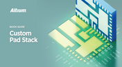
Custom Pad Stack Whitepaper

Explore our manual on the Custom Pad Stack enhanced feature. From thermal connections to pad shapes, every detail matters. Pads are no longer merely points; they demand unique, tailored solutions. With Altium Designer 24, you can customize pad shapes, fine-tune thermal relief, and master rounded/chamfered rectangle pads to meet manufacturing standards, conquer tight spaces, and elevate your design game significantly.

Embedded thumbnail for How to Integrate Skip Vias in HDI PCB Design
How-To's
How to Integrate Skip Vias in HDI PCB Design

Discover the intricacies of utilizing Skip Vias in HDI PCB design through this comprehensive guide. This video provides a step-by-step walkthrough on integrating skip vias into your high-density interconnect PCBs, delving into the advantages, disadvantages, and strategic applications to optimize electronic functionality.

Blog
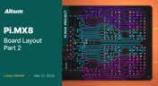
Pi.MX8 Project - Board Layout Part 2

We are continuing the exploration of board layout in our Pi.MX8 Project. In this chapter, we focus on defining the impedance profiles, establishing matching design rules for the correct trace width, and initiating the routing of the DRAM interface.

Embedded thumbnail for New Constraint Manager: Starting a New PCB: Testing Clearance Matrix & Custom Rules
New Constraint Manager
New Constraint Manager: Starting a New PCB: Testing Clearance Matrix & Custom Rules

Starting a new PCB project? Follow along as we guide you through essential steps, focusing on leveraging the Clearance Matrix and Custom Rules for precise design control. Unlock the full potential of Constraint Manager in Altium Designer 24 to kickstart your projects efficiently.

Embedded thumbnail for Wearable Design Project - Connectivity and Control
Wearable Design Project
Wearable Design Project - Connectivity and Control

Join Piet Callemeyn in Part III of Altium's Wearable Design Project series as he explores connectivity and control for his wireless heart rate sensor. Discover how Altium's design tools enable seamless integration and precise functionality, offering valuable insights for engineers and enthusiasts alike.

Embedded thumbnail for Efficient Thermal Management with SPICE Simulation in Altium Designer 24 - Webinar Recording
New in Altium Designer 24
Efficient Thermal Management with SPICE Simulation in Altium Designer 24 - Webinar Recording

Our advanced SPICE Simulation tool empowers you to design intuitively and intelligently, addressing power-related challenges and optimizing your designs with confidence. Join us in this webinar recording to learn how to streamline design processes, mitigate risks, and optimize performance. Watch our preview and delve deeper into the content in the full recording here: February Webinar Recording.

Embedded thumbnail for PCB Section View: Use Cases
New in Altium Designer 24
PCB Section View: Use Cases

Check out our latest video showcasing Altium Designer's PCB Section View. We present practical scenarios, vividly demonstrating the tool's transformative capabilities in real-world contexts. Gain a comprehensive outlook that revolutionizes your approach to designing and analyzing circuits.

Blog
Constraint Manager Whitepaper

Explore the precision of PCB design with Altium Designer's latest Constraint Manager! Hone your skills in component positioning, routing, and rule definition to enhance your design capabilities with Altium's state-of-the-art tools. Discover more about this cutting-edge feature in the manual today.

Embedded thumbnail for Mastering Octopart - Get to Know Octopart.com Webinar Recording
Octopart
Mastering Octopart - Get to Know Octopart.com Webinar Recording

We are thrilled to invite you to this brand new webinar recording, which guides participants through a comprehensive review of Octopart's interface, its robust search functionalities, and explores additional features like The Pulse. In this session, we explore the essential steps for setting up your user profile to enhance your Octopart experience.

Blog
USB to Serial-Over-RJ45 Module

Have you considered converting a USB interface to serial (UART), while delivering data over a custom Ethernet cable and RJ45 connectors? If so, we invite you to check out this article on building a USB to Serial-Over-RJ45 Module. Additionally, you'll find a link to our workspace to explore the entire project.

Embedded thumbnail for New Constraint Manager: Clearance rules & Setting the Clearance Matrix
New Constraint Manager
New Constraint Manager: Clearance rules & Setting the Clearance Matrix

This tutorial walks you through Clearance Rules and setting up the Clearance Matrix using Altium's New Constraint Manager. Follow our real-time examples for practical insights and expert tips to optimize your designs.

Blog
Pi.MX8 Project - Board Layout Part 1

Our exploration of the Pi.MX8 open-source computer module project progresses. In this third chapter, our focus shifts to the PCB layout preparation of the board. Key topics include defining the layerstack and component break-out routing.

Tag
Article preview
Blog
PCB Via Current-Carrying Capacity: How Hot is Too Hot?

Trace and via current-carrying capacity are legitimate design points to focus on when designing a new board that will carry high current. The goal is to keep conductor temperatures below some appropriate limit, which then helps keep components on the board cool.
Blog
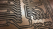
How to Maximize Copper in Your PCB Design: The Pros and Cons of Copper Pouring Versus Placing

There is a saying in copper pour PCB design, “Copper is free.” It means a PCB editor designer must think in reverse. A board starts off as solid copper, and the copper you don’t want is removed. It is faster to build, less consumptive, and less expensive to make a board that is mostly copper as compared to the same size board that is mostly bare. Picking the correct technique will make the difference between an effortless or frustrating experience.

Article preview
Blog 5月 14, 2020
How to Highlight Nets in Altium Designer to Simplify Schematic and PCB Designs

Highlighting nets will help you simplify your schematic and PCB design. In Altium , there are multiple options that enable you to leverage this capability to simplify the verification of connections and circuit paths and make sure that the design you send to your manufacturer accurately reflects the printed circuit board you need built.

Routed tracks
Blog 5月 5, 2020
Helpful Tips for Interactive Routing in Altium Designer

Before you jump into the software, you should know the types of things you’re going to want to look out for. Traces, connection lines, differential pair routing, and route paths can all affect the routing process of your board. Make sure that you’re equipped knowing, ultimately, what you want your board design to accomplish and furthermore, where you anticipate potential problem areas to be.

Blog 4月 22, 2020
Any Angle Routing: When Should You Use It?

EDA tools have come a long way since the advent of personal computing. Now advanced routing features like auto-routers, interactive routing, length tuning, and pin-swapping are helping designers stay productive, especially as device and trace densities increase. Read full article in our blog:

Blog 3月 20, 2020
A Message from Altium on COVID-19

We understand that many of you, like ourselves, have transitioned to working remotely. This process comes with its challenges and we would like to offer all and any help we can to minimize disruptions for your teams and business.

Blog 3月 2, 2020
About Altium Designer Home Page

With the new Altium Designer Home page, we are aiming to help users stay up to date with the latest features and productivity tricks available in Altium Designer. Learn more about the Home page in this documentation article.

altium-community-forum
Blog 2月 25, 2020
Getting Connected: Altium’s User Community Forums

The Altium design environment is a complex and sophisticated set of software tools. Not surprisingly, becoming proficient with these tools will take some time, and you’ll need to practice every step of the design process from beginning to end. So what happens if you get stuck along the way?


Tag
NEW
Embedded thumbnail for A fraction of a millimeter is the difference between a robot that fits and one that doesn't
Collaborative Engineering with Team Ribbot
A fraction of a millimeter is the difference between a robot that fits and one that doesn't

Check out the latest episode about Team Ribbot and see how they move design data between their electrical and mechanical tools without losing accuracy. Discover how Altium Designer and MCAD CoDesign help bring the boards, housings, and custom motors together right the first time with no surprises.

NEW
Embedded thumbnail for  HDI PCB Stackup Breakdown - Etching Weight Via Spacing, & More
How-To's
HDI PCB Stackup Breakdown - Etching Weight Via Spacing, & More

HDI PCB design depends on getting the stackup and manufacturing constraints right. In this deep dive, we examine a real HDI audio-interface board and explore common pitfalls, from how copper weight and etching affect minimum clearances to why solder mask slivers below 1 mil can cause manufacturing issues. You’ll also learn how proper board-edge clearance and copper pullback help protect SMD pads during routing.

Embedded thumbnail for  How do you review a robot design when your team is never in the same room?
Collaborative Engineering with Team Ribbot
How do you review a robot design when your team is never in the same room?

Team Ribbot’s engineers are spread across five states and juggle full-time jobs while building a 250-pound combat robot in their spare time. Discover how Altium Designer and Altium 365 keep the team connected, letting engineers open the live design from a laptop or phone, inspect the board in 3D, and leave comments directly on the design.

Embedded thumbnail for  Improve Visual Accuracy with True Arcs
New in Altium's Software
Improve Visual Accuracy with True Arcs

Discover how True Arc Rendering improves arc visualization in the PCB Editor and PCB Library Editor by displaying true arcs across 2D, 3D, and Board Planning modes. This provides a more accurate representation of board geometry and helps you work with curved features with greater precision throughout the design process.

Embedded thumbnail for Two engineers, one board, nobody's work gets wiped out
Collaborative Engineering with Team Ribbot
Two engineers, one board, nobody's work gets wiped out

When Team Ribbot’s electrical and mechanical engineers work on the same combat-robot design, unwanted changes can mean hours of lost work. See how Altium Designer and MCAD CoDesign let the team review and selectively accept changes, enabling seamless parallel collaboration across different locations and schedules.

Embedded thumbnail for Visualize and Refine Your Harness Designs
New in Altium's Software
Visualize and Refine Your Harness Designs

Create detailed views of bundle contents, control wire and cable paths, and rotate physical models to accurately represent the final harness assembly. These capabilities give you greater control over harness design and help ensure your digital model reflects the physical result.

Embedded thumbnail for Introducing Agentic Requirements Engineering
New in Altium's Software
Introducing Agentic Requirements Engineering

Discover a new way to work with Requirements Portal through Agentic Requirements Engineering. AI agents analyze your project data and surface proposals for your approval, reducing friction in requirements management and helping align your team's shared model with your design intent.

Embedded thumbnail for Simplify Rule Set Updates and Replacement
New in Altium's Software
Simplify Rule Set Updates and Replacement

Learn how to import rule sets with greater flexibility in Altium. When importing rules, you can add new rules to your existing set, replace only rules that match, or completely replace the current rule set giving you full control over how design rules are updated.

Embedded thumbnail for  How Team Ribbot fits 40 kW of power into a 250-pound combat robot
Collaborative Engineering with Team Ribbot
How Team Ribbot fits 40 kW of power into a 250-pound combat robot

What do you get when you pack the power of a small electric car into a combat robot with virtually no room to spare? In the first episode of our collaboration with Team Ribbot and Altium, explore how seamless ECAD-MCAD collaboration helps the team tackle complex design challenges, optimize high-performance designs, reduce errors, and bring products to life faster.

Embedded thumbnail for Just Released: Supplier Data Merging
New in Altium's Software
Just Released: Supplier Data Merging

Discover how the Supplier Data Merging feature brings together supplier information from your custom parts database and the Altium Parts Provider into a single, unified view. Access consolidated supplier data wherever supplier part numbers appear, including in ActiveBOM and during component selection.

Embedded thumbnail for How Altium’s Layer Stack Manager Actually Works
How-To's
How Altium’s Layer Stack Manager Actually Works

Take a look inside Altium's Layer Stack Manager and discover how its impedance calculator determines the ideal trace width for your target impedance. In this video, we break down the "black box" behind the calculation and show how the Simbeor-based field solver provides accurate results while eliminating the need for advanced field solver expertise.

Embedded thumbnail for Connect Requirements Directly to Your PCB Design
New in Altium's Software
Connect Requirements Directly to Your PCB Design

See how the Requirements Portal integration in Altium Designer simplifies requirements management by bringing system requirements directly into your PCB design workflow. Connect requirements to design documents, assign tasks, track verification in real time, and keep your entire team aligned with seamless synchronization in Altium 365.

Embedded thumbnail for SFP Connector Routing: High-Speed Differential Pair Design Tips
How-To's
SFP Connector Routing: High-Speed Differential Pair Design Tips

Discover practical SFP and SFP+ routing tips in our latest video, inspired by a real question from the Altium subreddit. We cover how aggressive serpentine length tuning can be, how to reduce impedance discontinuities in tight meanders, and how meandering influences mode conversion at 10G and higher data rates.

Embedded thumbnail for Handle High-Density PCB Layouts with Ease
New in Altium's Software
Handle High-Density PCB Layouts with Ease

Push the limits of PCB design with support for up to 128 signal layers, empowering the development of even the most complex, high-density boards.

Embedded thumbnail for Skip Layer Routing for RF: Control Impedance & Cut Insertion Loss
How-To's
Skip Layer Routing for RF: Control Impedance & Cut Insertion Loss

Discover our latest video and learn how RF designers use a deeper ground plane to minimize skin-effect resistance, improve signal integrity over long high-frequency routes, and optimize impedance matching for oversized SMT pads in antenna launches and coaxial connectors.

Embedded thumbnail for Just Released: ODB++ Intellectual Property Protection
New in Altium's Software
Just Released: ODB++ Intellectual Property Protection

ODB++ Intellectual Property Protection lets you control exactly what design data is included in the ODB++ output, ensuring each manufacturing partner receives only the information needed for their specific fabrication or assembly tasks.

Tag
Your search returns no results.