News & Updates


Blog
•
DC-Aware Return Current in Mixed Signal PCBs
In this article, we will examine specific cases involving these types of components, where a very low-frequency signal or a DC signal needs to be measured, and the return path must be tracked to ensure the current loop is tight.


Blog
•
PCB Layout Replication: The Perfect Tool for Test Jigs
Replicate your circuits across multiple blocks with just a few clicks using a flawless preview pane, ensuring consistent, perfect results without the need for trial and error. Check out our new article on the PCB Layout Replication feature.


Blog
•
Durability of Pin Plating Materials for PCB Connectors
Pin headers are common components in PCBs, yet one specification often overlooked is the plating material. Discover more about plating materials for electrical connectors in our latest article.


Blog
•
4 Reasons Why We Chose AWS GovCloud (US) for Altium 365 GovCloud
In this blog, we explain the reasons behind our decision to operate Altium 365 GovCloud within AWS GovCloud (US). This partnership is guided by a clear vision: to provide our users with a secure, compliant, and reliable platform for sensitive electronics design data.



Blog
•
How to Reduce Noise From Magnetostriction in Magnetic Components
Magnetic components driven by an AC signal can exhibit an irritating property due to magnetostriction - an effect causing vibrations in magnetic materials, resulting in audible sound. Explore this phenomenon further and discover methods to minimize its impact.


Blog
•
3D MID Design Whitepaper
Dive into a dynamic design experience where you can visualize and edit your circuits in true 3D, offering unparalleled precision. Altium Designer's 3D-MID (Mechatronic Integrated Device) Design tool revolutionizes the design process, providing a fresh perspective. Explore the capabilities and benefits of this feature in our comprehensive guide.

Blog
•
Types of Wiring Harnesses for Electronics
In today's world, many products utilize multiple PCBs interconnected with each other, often leading to a complex network of cables within an enclosure. The most effective way to manage these wires and cables is by constructing a wiring harness. This article explores the various types of harnesses used in electronics.


Blog
•
5 Advantages of Z2Data Integration You Can't Ignore
Z2Data Integration in Altium 365 offers a practical way forward for engineering and procurement. Here are the top five advantages that can streamline your workflows.
Blog
•
Leveraging Altium Designer's Capabilities: Transforming PCB Design Data Management
Are you curious about how Altium Designer's PLM integration is revolutionizing electronics design? Bid farewell to inefficiencies and expensive revisions, and embark on discovering the cutting-edge approach to managing design data. Dive into our latest article to learn how to leverage this new standard in design data management.
Blog
•
Start Altium Designer 24 Training for Free
Level up your design skills with Altium Designer 24 training! Whether you're looking to brush up on the basics or delve into advanced techniques, our instructor-led or on-demand videos will help you master the latest features.

Blog
•
How Altium 365 Supports Agile Hardware Development
Discover how Altium 365 can be your ally in making agile hardware development a practical reality.
Blog
•
Constraint Manager Whitepaper
Explore the precision of PCB design with Altium Designer's latest Constraint Manager! Hone your skills in component positioning, routing, and rule definition to enhance your design capabilities with Altium's state-of-the-art tools. Discover more about this cutting-edge feature in the manual today.
Blog
•
Redefining the Assembly Process for Miniaturization and Ultra HDI Technology
Learn the whole story of revamping the SMTA Test Board, the groundbreaking tool for solder paste testing.
Blog
•
Why the Principles Are Sound, but the Tactics Need a Re-Think
Explore common principles and rituals of Agile and how you can adapt them to hardware product development.

Blog
•
USB to Serial-Over-RJ45 Module
Have you considered converting a USB interface to serial (UART), while delivering data over a custom Ethernet cable and RJ45 connectors? If so, we invite you to check out this article on building a USB to Serial-Over-RJ45 Module. Additionally, you'll find a link to our workspace to explore the entire project.

Blog
•
Why the Principles Are Sound, but the Tactics Need a Re-Think
Explore common principles and rituals of Agile and how you can adapt them to hardware product development.

Blog
•
Pi.MX8 Project - Board Layout Part 1
Our exploration of the Pi.MX8 open-source computer module project progresses. In this third chapter, our focus shifts to the PCB layout preparation of the board. Key topics include defining the layerstack and component break-out routing.

Blog
•
PCB CoDesign Whitepaper
Design faster together with the innovative PCB CoDesign feature, exclusively available in Altium Designer. This cutting-edge functionality seamlessly integrates schematic and PCB design, facilitating concurrent work by multiple engineers on the same project. Learn more about this groundbreaking feature in our comprehensive manual.

Blog
•
How to Test Suspect Electronic Components
Electronic components power nearly everything in our modern lives. However, as long as there are buyers for parts, counterfeiters will persist in their endeavors. Financial losses resulting from fake components are challenging to ascertain due to enforcement limitations and the difficulty in collecting data on the issue. In this article, we demonstrate how to test and verify components in batch orders.

Blog
•
The Positive Impact of Supply Chain Visibility on Design to Cost
With increased electronics supply chain visibility, you can develop better products faster and align perfectly with budget constraints early on. Here’s why.

Blog
•
What Most Agile "Gurus" Get Wrong About Hardware Development
Explore common myths about Agile hardware development and learn how to adapt Agile principles for hardware projects.

Blog
•
Design Phase – Lid Assembly Electronics Part 2
We are going deeper into lid assembly electronics in our Open Source Laptop project. In this chapter we will tackle the PCB design of the webcam board and show you how to deal with some expected challenges, such as overall small form factor of the board or breaking out the microscopic webcam image sensor.

Blog
•
Compare Commercial Altium 365 vs Altium 365 GovCloud
If you're trying to understand how commercial Altium 365 differs from Altium 365 GovCloud, you're in the right place. Click to grasp the unique features of each.

Blog
•
5 Ways Hardware Development Is Just… Different
Explore the challenges and strategies of implementing Agile methodology in electronics hardware development. Understand key differences between hardware and software development within the Agile framework.

Blog
•
Flexible Circuit Assembly: Thinking Through Component Placement
The flexible circuits are ideal for applications where a thin, small, and lightweight PCB is needed. However, in such cases, challenges in assembly and fabrication often arise. This article delves into these challenges, focusing on component selection and placement and how they can significantly impact the performance of the flexible circuit in its intended application.
Blog
•
Coding Your Own Networked Test Equipment
Have you ever performed manual tests? If your answer is yes, you're likely aware of how laborious and time-consuming the entire process can be. Allow us to introduce you to the realm of test equipment automation. Our new step-by-step guide empowers you to write code that seamlessly configures your networked test equipment, all from the convenience of your computer.
Blog
•
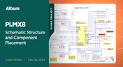
Pi.MX8 Project – Schematic structure and component placement
We are advancing with our brand new Pi.MX8 Project. In this chapter, we delve deeper into two crucial aspects: the overall schematic and component placement on the PCB board. Don't hesitate to check it out. Additionally, you can follow this project through our workspace; the link is provided within the article.
















Your search returns no results.


