News & Updates

Blog
•
Your Design Data Has Zero Defense
Your design data may be more exposed than you think. This webinar shows how to identify common security gaps and secure engineering workflows with centralized access control and governance.

Blog
•
Flex Circuit Coverlay: Design with Lamination Processes In Mind
Your flex PCB may look perfect in CAD but coverlay doesn't stay perfectly still during manufacturing. This article reveals why designing for lamination behavior is one of the most important steps in building reliable flex circuits.

Blog
•
Integrated PCB Design vs. Legacy Point Tools: What’s the Real Cost?
As hardware development grows more collaborative, disconnected point tools can introduce data inconsistencies, traceability gaps, and costly coordination challenges. This article examines how integrated PCB design environments connect design, mechanical, supply chain, and review workflows to improve efficiency throughout the product lifecycle.

Blog
•
Make Better Design Decisions with Signal and Power Integrity Insight
Signal integrity and power integrity are closely connected, with problems in one often affecting the other as designs become faster and more complex. This webinar explains how integrated analysis workflows help engineers evaluate PDN performance, identify potential issues early, and improve overall design quality.

Blog
•
Optimizing Your Electronics Product Design Workflow and Eliminating Bottlenecks
Every manual handoff adds time and risk to the product development process. This article shows how modern design workflows automate routine tasks, improve data visibility, and help engineering teams focus on innovation instead of administration.
Blog
•
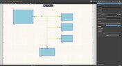
Avoid Cross-Board Signal Integrity Issues in High-Performance Multiboard PCB Designs
Your signal may be perfect on the PCB and fail the moment it crosses a connector. This article explores the hidden SI challenges in multi-board systems and how engineers can eliminate them before they become costly debugging sessions.

Blog
•
Proto-BOM in Minutes: How BOM Portal Accelerates Component Selection
Still building BOMs the hard way? Discover how modern workflows can help you create a prototype-ready BOM faster while improving visibility into pricing, availability, and risk.

Blog
•
How to Manage Power Integrity and EMI in Complex Multiboard Systems
This article examines the challenges of maintaining power integrity and controlling EMI in complex multiboard systems. It provides practical strategies for managing return paths, connector transitions, and power distribution across interconnected assemblies.

Blog
•
Agile Teams: From Design Tool to Product Development Platform
Learn how Agile Teams evolves beyond traditional PCB design workflows to support connected product development. This webinar explores how centralized data, collaboration tools, and governance capabilities help teams accelerate delivery while maintaining control.

Blog
•
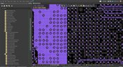
Benefits of Using an Integrated Design Environment for PCB Development
Using separate tools often creates inefficiencies and increases the risk of mistakes. This article explains how integrated design environments streamline workflows by keeping design data connected and accessible.

Blog
•
Enterprise vs. Midsize PCB Design Software: What Actually Changes at Scale
PCB design challenges change significantly as organizations scale. This article explores the key differences between mid-size and enterprise design environments, from collaboration and governance to data management and workflow automation.


Blog
•
BOM Portal vs BOM Tool: What Changes When You Upgrade
Not all BOM solutions work the same way. This article explains the key differences between BOM tools and BOM portals, and why real-time data and collaboration are becoming essential for modern electronics development.
Blog
•
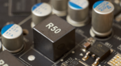
How to Combat Power Supply EMI in Your PCB
Power supplies are one of those systems we all tend to take for granted. Everyone’s first task in power supply design is usually to ensure the voltage and current output reach the desired level, probably followed by thermal considerations. However, due to safety issues, EMC requirements, the use of higher PWM frequencies, and the need for smaller packaging, power supply EMI should be a major design consideration. With that being said, what are the major sources of power supply EMI, and how can power supply designers keep them in check?
Blog
•
Leveraging the Free Footprint Community to Design at Lightning Speed
Designing footprints is a job most people hate. It’s tedious, time-consuming, and doesn’t result in much except, well, a footprint. Companies now realize this pain point and offering designers free, well-designed PCB footprints. Why would they spend their time doing this? In this article, we’re going to review some of the free offerings that exist within the PCB design community. Once you’re armed with this information, you will spend most of your time designing and routing boards instead of pulling your hair out creating footprints all day.

Blog
•
Designing for Multiple PCBs in the Same Project
The majority of our PCB designs sit as a single PCB under our Altium Designer projects. It sometimes happens that we have a single project that requires multiple PCBs with various stuffing options, but when it happens, a lot of us tend to get stuck. How do you handle the exact change across both projects? How do you guarantee those changes to be identical? This article will review an approach to managing multiple PCB designs within a single project, ensuring your single source of truth.

Blog
•
Designing 5G Devices
The next stage in the evolution of mobile telephony is here with the roll-out of 5G. The designer looking to incorporate functionality to handle 5G signals into their circuits will face some challenging issues. So, what’s so special about 5G?

Blog
•
All About Your PCB Trace Length: How Long is Too Long?
The maximum PCB trace length you can place between two components depends on multiple factors, such as signaling protocol, component specification, losses in PCB laminate, and skew. With all this in mind, let’s look at where losses accumulate along the channel.
Blog
•
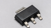
Using an LDO vs. Switching Regulator in Your PCB
For low power devices, we generally see two types of power regulators: a low dropout regulator (LDO) or a switching regulator. You can mix and match these at different points along your power bus, but there’s still the matter of choosing whether to use an LDO vs. a switching regulator in your designs. If you’ve ever wondered how these decisions are made and when to use each type of regulator, just know that there is more to this decision than simply looking at the input/output voltage/current.

Blog
•
What They Don’t Teach You About Fluxes
PCB fabrication is an extremely complex technological topic that deserves recognition as the most fundamental part of PCB engineering. Unless connectors, conductive adhesive, wire-bonding, or zebra-tape are used, in the modern electronics industry it’s always necessary to use some kind of flux during the soldering process to create an electric connection. In this article, we’ll discuss fluxes — what they are, what they are made of (yes, there is going to be a lot of chemistry, don’t be scared), how they should be used, and in what direction the industry is going.
Blog
•
Thermal Management for Integrated Circuits
As anyone who designs and builds electronic devices knows, the device will generate heat when it’s switched on. Wherever current flows through an impedance, energy losses will manifest themselves as heat. Integrated circuit packaging is getting smaller to meet the trend for more compact devices but at the cost of poorer thermal properties. This article describes the basic thermal management approaches to consider in your next designs.

Blog
•
Anatomy of Latitude Part Two: "Thread with a Needle” in the context of energy
We continue to explore the magic of energy conversion in a PWM transducer. Why is it magic? Theoretically, in a PWM transducer this happens without losses, isn't that magic? A PWM transducer, like a tailor with scissors, cuts the “fabric of energy” into pieces, and then, like a sewing machine, stitches the pieces of energy into a dress - DC Magnitude. What is a constant component and how can we get it? Let's explore!
Blog
•
Anatomy of Latitude Part One: Pulse Width Modulation (PWM) as a Result of the Evolution of Linear Systems
There are different techniques in the world of technology to achieve various goals, both final and intermediate. Some techniques are so successful that they are commonly used with high efficiency. Electronics is no exception. The greatest example is the use of Pulse Width Modulation (PWM) signals (energy), which is applied in any modern electronic device. To apply PWM effectively, it is necessary to understand the engineering difficulties that engineers faced in the past, and the thoughts and ideas that subsequently were combined into effective, complete PWM power solutions.
Blog
•
What Influences Electrolytic Capacitor Lifespan?
If you speak with a bunch of design engineers, you might quickly form the opinion that the electrolytic capacitor has a particularly dubious reputation. A faulty electrolyte mix used in these types of capacitors led to premature device failures, and quite often, a “bit of a mess” was made to the PCBs on which they were soldered. However, despite the problem of the capacitor plague, this article is focusing on helping the designer understand how to get many more years of useful life from an electrolytic capacitor.

Blog
•
Creating Elegant and Readable Schematics
A schematic drawing will not only tell your PCB design software what needs to connect where, but it also communicates the purpose of a circuit to other people. It’s easy to create a schematic, but it can be harder to make a helpful schematic that can be quickly and easily read and comprehended by the reader. In this guide, based on years of industry experience, we will show you how to improve your schematic layout so that your designs are elegant and readable.

Blog
•
Must Have Rapid Prototyping Tools
Suppose your job involves rapidly iterating designs or creating a wide variety of products for clients. In that case, there are some essential tools available that can save you a tremendous amount of time, bringing high engineering risk devices to completion successfully. Whether you’re working on internal projects or developing high mix devices for clients as a consulting or freelance firm, these indispensable tools will help you ship a higher quality product in less time.

Blog
•
Best Practices for Sharing PCB Files vs. Sharing PCB Projects
Even though today’s cloud platforms are immaculately secure and they allow a range of files to be easily shared, there are times where you should limit the data you’re sharing to only the critical files required. For PCB designers, this means either sharing entire design projects or sharing individual files with your manufacturer, customers, contractors, or collaborators. If you want to eliminate liabilities and keep your team’s design data secure, consider these best practices for sharing PCB design data with Altium 365.

Blog
•
Best Practices for Using Reference Designs
Best component companies will release reference designs for their new and legacy products to show designers an example application for a component. If the reference design is good enough and it very nicely illustrates how to quickly engineer around a few main components, I’m likely to use them in the design and the component maker has just earned my business. If you’re a newer designer and you’re wondering whether reference designs are right for your next project, follow these best practices so that you don’t make any mistakes with your reference design.

Blog
•
Transmission Line Fundamentals And Electromagnetic Fields, Part 1
When we deal with “abstract” aspects of electromagnetic fields and how they function, it can be easy to get lost in the weeds regarding them. The first part of this article will address an important aspect of transmission line fundamentals, namely how electromagnetic fields and waves propagate on a transmission line. This article’s end goal is to create a core understanding of these concepts so that when it comes time to design a PDS, the proper design methodologies are followed and a properly working PDS is achieved appropriately, the first time and every time.


Your search returns no results.


