News & Updates

Blog
•
Your Design Data Has Zero Defense
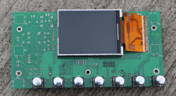
Your design data may be more exposed than you think. This webinar shows how to identify common security gaps and secure engineering workflows with centralized access control and governance.

Blog
•
Flex Circuit Coverlay: Design with Lamination Processes In Mind
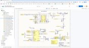
Your flex PCB may look perfect in CAD but coverlay doesn't stay perfectly still during manufacturing. This article reveals why designing for lamination behavior is one of the most important steps in building reliable flex circuits.

Blog
•
Integrated PCB Design vs. Legacy Point Tools: What’s the Real Cost?
As hardware development grows more collaborative, disconnected point tools can introduce data inconsistencies, traceability gaps, and costly coordination challenges. This article examines how integrated PCB design environments connect design, mechanical, supply chain, and review workflows to improve efficiency throughout the product lifecycle.

Blog
•
Make Better Design Decisions with Signal and Power Integrity Insight
Signal integrity and power integrity are closely connected, with problems in one often affecting the other as designs become faster and more complex. This webinar explains how integrated analysis workflows help engineers evaluate PDN performance, identify potential issues early, and improve overall design quality.

Blog
•
Optimizing Your Electronics Product Design Workflow and Eliminating Bottlenecks
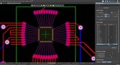
Every manual handoff adds time and risk to the product development process. This article shows how modern design workflows automate routine tasks, improve data visibility, and help engineering teams focus on innovation instead of administration.
Blog
•
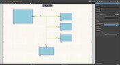
Avoid Cross-Board Signal Integrity Issues in High-Performance Multiboard PCB Designs
Your signal may be perfect on the PCB and fail the moment it crosses a connector. This article explores the hidden SI challenges in multi-board systems and how engineers can eliminate them before they become costly debugging sessions.

Blog
•
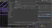
Proto-BOM in Minutes: How BOM Portal Accelerates Component Selection
Still building BOMs the hard way? Discover how modern workflows can help you create a prototype-ready BOM faster while improving visibility into pricing, availability, and risk.

Blog
•
How to Manage Power Integrity and EMI in Complex Multiboard Systems
This article examines the challenges of maintaining power integrity and controlling EMI in complex multiboard systems. It provides practical strategies for managing return paths, connector transitions, and power distribution across interconnected assemblies.

Blog
•
Agile Teams: From Design Tool to Product Development Platform
Learn how Agile Teams evolves beyond traditional PCB design workflows to support connected product development. This webinar explores how centralized data, collaboration tools, and governance capabilities help teams accelerate delivery while maintaining control.

Blog
•
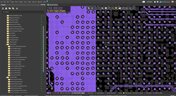
Benefits of Using an Integrated Design Environment for PCB Development
Using separate tools often creates inefficiencies and increases the risk of mistakes. This article explains how integrated design environments streamline workflows by keeping design data connected and accessible.

Blog
•
Enterprise vs. Midsize PCB Design Software: What Actually Changes at Scale
PCB design challenges change significantly as organizations scale. This article explores the key differences between mid-size and enterprise design environments, from collaboration and governance to data management and workflow automation.


Blog
•
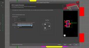
BOM Portal vs BOM Tool: What Changes When You Upgrade
Not all BOM solutions work the same way. This article explains the key differences between BOM tools and BOM portals, and why real-time data and collaboration are becoming essential for modern electronics development.

Blog
•
Ferrite Beads and Transfer Impedance in a PDN Simulation
The use of ferrites in a PDN is one design recommendation that is fraught with unclear guidance and over-generalized recommendations. If you see an application note or a reference design that recommends placing a ferrite in a PDN, should you follow this in your specific design, or should you ignore this and focus on adding capacitance?

Blog
•
Overview of PCB Design Output Files
Before your board can be put into production and prepared for assembly, you have to generate a set of files that assist your manufacturer. These are your PCB design output files, also known as manufacturing files, fabrication data, assembly files, and a host of other names. Before you send your design file off to a manufacturer in an email, make sure to get a list of their required fabrication and assembly files first. If you’re a new designer, take some time to read over the basic PCB manufacturing file extensions below.

Blog
•
Transformer Theory Made Simple
Transformers can provide very effective signal isolation and are used to manipulate AC voltage and current levels. They can achieve all this with a greater than 95% power efficiency, which is why we commonly see them used in bench power supplies, audio gear, computers, kitchen appliances, and wall-warts. However, transformer theory can be unintuitive and in this article we answer on questions about them
Blog
•
Using Altium 365 Over Your Vanilla Version Control System
There are all sorts of version control systems (VCS) out there that people have been using with their PCB design software. As discussed in Why Use a Version Control System, we looked at different options ranging for local hard drive storage to sophisticated online revisioning systems. In this article we will be reviewing the differences between a standard VCS and Altium 365.

Blog
•
Recover Conductor Losses By Clearing Your PCB Ground Layer
Controlled impedance routing at high frequencies is difficult enough, and it's important to make sure that you stay within your loss budget on long routes or in lossy media. When you have to route a long trace or a long differential pair to a connector or another component, what can you do if you're reaching the end of your loss budget? In this article, we’ll take a look at the skip reference routing method and explain how it can help recover some loss budget in a lossy interconnect.
Blog
•
Announcing SOC 2 Type 1 Certification for Altium 365
We are pleased to announce that Altium 365 is officially SOC 2 Type 1 certified. System and Organization Controls (SOC) 2 is a widely recognized attestation of security compliance defined by the AICPA and is considered the standard for ensuring data security and operational maturity. A SOC 2 certification provides valuable information for companies to assess the quality of the security provided by a service such as Altium 365.

Blog
•
Improving Supply Chain Success with BOM Management
It’s no secret that component shortages have become more frequent this year. Companies will continue to grapple with supply chain challenges into 2022 and beyond. The impact of manufacturing delays can be substantial if a part is not available. Delays occur and sales plans get put on hold. It can also be very expensive and risky to replace parts from multiple sources. Fortunately, many shortages can be avoided by introducing proactive supply chain practices.

Blog
•
Overview of PCB/PCBA Reliability and Failure Analysis
Reliability testing and failure analysis of a PCB/PCBA go hand-in-hand; when designs are stressed to the limit, their failure modes need to be determined through thorough inspection and analysis. To get started on this topic, it’s important to understand the qualification aspects that will govern your bare board design and the PCBA. We’ll look at the various dimensions of PCB/PCBA reliability, as well as some of the standard failure analysis techniques used to identify potential design change requirements.

Blog
•
When Do PCB Power Plane Resonances Occur?
By now, designers should be aware of some important behavior involved in power delivery to components in a PCB, particularly for digital components. All digital components produce and manipulate wideband signals, where the frequency content theoretically extends up to infinite frequency. As such, some radiation may propagate through your PCB, leading to resonant behavior that is not observed on the power rail.

Blog
•
How to Choose PCB Plating for Your Finished Board
Once your board passes through the standard PCB fabrication process, the bare copper in your PCB will be ready for the application of a surface finish. PCB plating is applied to protect any copper in your PCB that would be exposed through the solder mask, whether it’s a pad, via, or other conductive element. In this article, I’ll run over the different PCB plating material options and their advantages in your PCB.

Blog
•
What is the PCB Supply Chain?
The PCB supply chain encompasses multiple components, raw materials, and the PCB itself. PCBs and PCB assemblies are often the most technically complex components that are purchased for electronic assemblies and products. The complexity of modern PCBs leads to several challenges for a supply chain management team that may be significantly different when compared with other commodities the team manages. In this brief guide, we'll look in-depth at the PCB supply chain, and specifically what falls within the purview of a procurement and supply chain management team.

Blog
•
A Guide to Mode Conversion, Its Causes, and Solutions
On interconnects, such as board-to-board connections or cascaded transmission line arrangements, you have an important EMC compliance metric that is sometimes overlooked. This is mode conversion, which can be visualized in an S-parameter measurement for differential and common-mode signal transmission. In this article, we’ll look at a short overview of mode conversion in high-speed design with some examples from common differential standards.

Blog
•
PCB Via Size and Pad Size Guidelines
There are some aspects of PCB design and layout that seem deceptively simple, and yet they have a complex answer that is related to many important aspects of manufacturing. One of these design aspects is the match between PCB via size and pad size. Obviously, these two points are related; all vias have a landing pad that supports the via and provides a place to route traces into a via pad. However, there are some important sizing guidelines to follow when the matching pad and via sizes, and this match is an important element of DFM and reliability.
Blog
•
Differential Microstrip Impedance Calculator
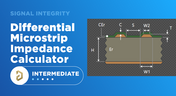
Are you looking for a free tool that you can use to calculate the impedance of differential microstrips? We created a simple tool you can use to calculate differential microstrip impedance for a given geometry and dielectric constant. If you’ve been looking for an accurate differential microstrip impedance calculator, then the calculator below is certainly one of the best free tools you’ll find on the internet before you start using field solvers to determine differential pair impedance.

Blog
•
Getting Through a PCB DFM Check
In this article, we’ll discuss the key design features to implement, and steps to take prior to fabrication that will help prevent some common DFM problems. I’ll also provide examples of where I commonly see these PCB DFM problems in signal integrity circuits.

Blog
•
What is Spreading Inductance?
If you’re working with a high-speed digital component, there are some simple power integrity rules that should be followed. However, there is one quantity that is sometimes ignored when building a PDN impedance simulation: the spreading inductance of your plane pair. Here are some points designers should know about the spreading inductance of a plane pair.


Your search returns no results.


